
INTRODUCTION
Wide-bandgap semiconductors are a fascinating class of materials which are distinguished by their wider energy bandgap (more than 3.2 eV) than conventional semiconductors such as silicon1, 2, 3. The bandgap represents the energy required to move an electron from the valence band to the conduction band, and a larger bandgap leads to unique electronic and optoelectronic properties1, 2, 3. This is the very characteristic that has propelled wide-bandgap semiconductors to the forefront of research and innovation, offering the potential to revolutionize various electronic and optoelectronic applications (Fig. 1).
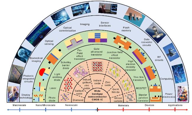
Fig. 1. Detailed summary of wide bandgap semiconductors based on materials, devices, and application perspective. |
Several noteworthy wide-bandgap semiconductors, including silicon carbide (SiC), gallium nitride (GaN), zinc oxide (ZnO), indium oxide (In2O3), indium-gallium-zinc-oxide (IGZO), gallium oxide (Ga2O3), aluminum nitride (AlN) and diamond, exhibit various intriguing properties such as high electron mobility, high breakdown voltage, high thermal conductivity, excellent optical absorption, and efficient light emission (Table 1). These properties lay the foundation for the fabrication of diverse electronic and optoelectronic devices (Fig. 1).
Table 1. Properties of wide bandgap semiconductors. |
| Property | 4H-SiC | GaN | ZnO | In2O3 | IGZO | Ga2O3 | Diamond | AlN |
|---|---|---|---|---|---|---|---|---|
| Bandgap (eV) | 3.3 | 3.4 | 3.37 | 3.7 | 3.5 | 4.9 | 5.5 | 6.0 |
| Breakdown field (MV/cm) | 3.1 | 4.9 | 0.01 | NA | 2.7 | 10.3 | 4.4 | 15.4 |
| Sat. velocity (107 cm/s) | 2.2 | 1.4 | 3.2 | 0.25 | 0.8 | 1.8 | 1.5 | 1.6 |
| Thermal conductivity (W mK−1) | 490 | 230 | 50 | 2.2 | 1.4 | 13 | 2200 | 320 |
| Johnson FOM ratio vs Si | 278 | 1089 | NA | NA | NA | 2844 | 81 000 | 7744 |
| Baliga FOM ratio vs Si | 712 | 3170 | 10 | NA | 3.7 | 4125 | 62 954 | 38 181 |
| Tunneling eff. mass (mo) | NA | 0.15 | 0.24 | 0.40 | 0.34 | 0.31 | 0.69 | NA |
| Melting point (°C) | 2730 | 2500 | 1975 | 1910 | 850 | 1700 | 3550 | 2830 |
| Thermal budget | High | High | Low | Low | Low | High | High | High |
| CMOS demonstration status | Cree 2006 | HRL 2016 | NA | NA | NA | NA | NA | NA |
Electronic devices:
•Bipolar junction transistors (BJTs): wide-bandgap BJTs can operate at higher temperatures and voltages, making them suitable for high-power applications4.
•Metal-oxide-semiconductor field-effect transistors (MOSFETs): wide-bandgap MOSFETs enable high-frequency operation and reduced switching losses5.
•High electron mobility transistors (HEMTs): GaN-based HEMTs exhibit excellent RF performance and are used in radar systems, satellite communication, and cellular base stations6.
•Thin film transistors (TFTs): TFTs are essential for flat-panel displays, wearable electronics, and flexible devices7.
•Junction field effect transistors (JFETs): JFETs based on wide-bandgap materials are applied in harsh environments and high-power circuits8.
•Gate-all-around transistors (GAA): GAA designs enhance electrostatic control and reduce leakage current9.
Optoelectronic devices:
•Light-emitting diodes (LEDs): wide-bandgap semiconductors enable efficient and high-brightness LEDs, which are used in lighting, displays and signage10.
•Lasers: GaN-based lasers are integral to various applications, including medical procedures, optical communication, and materials processing11.
•Photodiodes: efficient photodetectors are crucial for optical communication, imaging, and sensing12.
These diverse devices can be integrated homogeneously and heterogeneously to create versatile wide-bandgap semiconductor integrated circuits (ICs). Integrating various devices on a single chip enhances overall functionality and performance. Wide-bandgap semiconductor ICs are applied in numerous electronic and optoelectronic domains (Fig. 1).
Electronic applications:
•Power electronics: wide-bandgap devices enable higher energy efficiency, power density, and higher operating temperatures in converters, inverters, and motor drives13.
•Computing: high-speed switching capabilities of wide-bandgap transistors enhance computing performance14.
•RF circuits: high-frequency operation and efficient power handling are essential for wireless communication systems15.
•Data converter circuits: enhanced speed and precision of analog-to-digital and digital-to-analog converters16.
•Flash memory: wide-bandgap memory devices exhibit faster read and write speeds, longer lifespan, and lower power consumption17.
•Sensor interfaces: wide-bandgap devices improve sensor sensitivity and interface capabilities18.
Optoelectronic applications:
•Imaging: wide-bandgap devices enable high-resolution and high-sensitivity imaging systems for scientific, medical, and industrial applications19.
•Optical communication: high-speed, efficient optical devices are vital for data transmission in modern communication networks20.
•Optical sensing: wide-bandgap photodetectors provide accurate and reliable sensing solutions for environmental and industrial monitoring21.
•Biomedical imaging: high-quality imaging devices contribute to advances in medical diagnostics and researches22.
•Photonic integrated circuits: wide-bandgap materials enable compact and efficient photonic circuits for data processing and communication23.
•Display technology: energy-efficient displays with improved color accuracy and resolution are achieved with the adoption of wide-bandgap devices24.
The remarkable properties of wide-bandgap semiconductors have facilitated the development of a diverse range of electronic and optoelectronic devices (Table 1). These devices can be integrated into versatile circuits, offering enhanced performance and functionality. Among the myriad applications, power electronics stands out as an exemplary domain that showcases the transformative impact of wide-bandgap semiconductor integrated circuits in improving the energy efficiency and power management.
This can be primarily attributed to the superior material properties exhibited by them in comparison to silicon25. The principal benefit of wide bandgap (WBG) semiconductors is their capacity to function at elevated temperatures, which leads to augmented power density and superior efficiency26. SiC devices have the capability to function at temperatures as high as 600 °C, whereas devices based on silicon are restricted to approximately 150 °C26. Utilizing smaller heat sinks and cooling systems allows for the downsizing of power electronics, resulting in a more condensed and compact form. WBG semiconductors exhibit a higher breakdown voltage, thereby enabling them to endure higher electric fields prior to experiencing a breakdown. The outcome results in an increased capacity to handle the voltage and enhanced dependability, rendering them well-suited for high-voltage implementations such as electric automobiles, sustainable energy infrastructures, and power networks25-27.
The escalating need for power control circuits that are more efficient and rely on WBG materials has been observed25-27. The integration of power transistors and CMOS IC in a monolithic manner is gaining popularity as a viable solution to address the demand28. The aforementioned methodology facilitates the development of power regulation circuits that provide a notable level of efficacy, compactness, and economical feasibility28. The regulation of current flow is achieved through the utilization of power transistors, whereas the control of power transistors is facilitated by CMOS ICs. Monolithic integration offers the notable benefit of obviating the requirement for distinct components2,29. The simplification of the circuit results in a reduction of its complexity, thereby facilitating its design and production2,29. In addition, the integration of monolithic components results in notable enhancements in the performance of the circuit. The enhanced efficiency of the circuit is attributed to the reduction of parasitic capacitance and inductance through the amalgamation of power transistors and CMOS ICs.
Monolithic integration is endowed with the benefit of facilitating the development of power control circuits that exhibit a high degree of dependability29. The integration of power transistors and CMOS ICs on common substrates leads to a reduction in susceptibility to thermal and mechanical stress for the circuit2,29. Enhancement of the circuit's durability renders it appropriate for deployment in hostile surroundings. The integration of monolithic components results in notable enhancements in power dissipation. The reduction of circuit resistance and consequent minimization of power dissipation as heat is attributed to the amalgamation of power transistors and CMOS ICs. This enhances the energy efficiency of the circuit and mitigates the necessity for cooling mechanisms2,29. Although monolithic integration offers numerous benefits, it is imperative to acknowledge its associated limitations. A primary limitation pertains to the intricacy of the production procedure29. The process of monolithic integration fabrication is intricate and necessitates specialized equipment and expertise. The escalation of manufacturing expenses may impede the extensive acceptance of this technology30,31. Subsequently, it was recognized that implementing CMOS technology utilizing WBG semiconductors presents significant challenges28. The major limitation is the lack of p-type metal-oxide-semiconductor field-effect transistors (p-MOSFETs)28. Consequently, there exists a significant need to suggest novel approaches for the advancement of WBG CMOS devices, which can facilitate the realization of monolithically integrated WBG intelligent power integrated circuits (ICs)28. This review aims to provide a comprehensive overview of the advancements made in ICs with the adoption of various WBG semiconductors, including SiC, GaN, ZnO, IGZO, In2O3, Ga2O3, and diamond.
OVERVIEW OF DIGITAL INTEGRATED CIRCUITS
Digital integrated circuits deal with discrete signals, specifically binary values, which are ‘0’ and ‘1’. These circuits employ various digital components like logic gates, multiplexers, flip-flops, encoders, and decoders.
Logic gates
In digital electronics, logic gates are fundamental components that perform logical operations on binary signals, which can be either ‘0’ (low level) or ‘1’ (high level). These gates follow the principles of Boolean algebra and could help manipulate these binary signals.
NOT gate (inverter) The NOT gate, symbolized by a bar over an input variable, essentially flips the state of the input. If the input is ‘0’, the output is ‘1’, and vice versa. The symbol for this gate can be seen in Fig. 2.
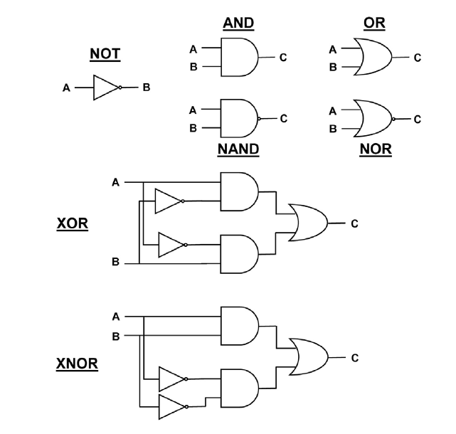
Fig. 2. Summary of logic gates including NOT, AND, NAND, OR, NOR, XOR, and XNOR equivalent circuits. |
AND gate The AND gate (Fig. 2), represented by a dot (‘·’), takes two inputs. It only produces a ‘1’ at the output when both inputs are ‘1’. If any input is ‘0’, the output is ‘0’.
OR gate In contrast, the OR gate (Fig. 2), denoted by a plus sign (‘+’), also takes two inputs. It outputs ‘1’ if at least one input is ‘1’. It produces ‘0’ only when both inputs are ‘0’.
XOR gate (exclusive OR) The XOR gate (Fig. 2), symbolized by a circle with a plus inside (‘⊕'), also has two inputs. It is different from the OR gate in the fact that it outputs ‘1’ when exactly one input is ‘1’, but ‘0’ when both inputs are the same (‘0’ or ‘1’).
Complementary logic gates Now, we have the complementary gates:
•NAND gate (NOT AND): this is essentially an AND gate followed by a NOT gate. It outputs ‘0’ only if both inputs are ‘1’. Otherwise, it produces ‘1’. NAND gates (Fig. 2) are versatile and can represent any logic function.
•NOR Gate (NOT OR): similar to the OR gate, a NOR gate (Fig. 2) followed by a NOT gate gives you this. It outputs ‘1’ only when both inputs are ‘0’. NOR gates are also capable of representing any logic function.
•XNOR Gate (Exclusive NOR): this is an XOR gate followed by a NOT gate. It outputs ‘1’ when both inputs are the same (‘0’ or ‘1’) and ‘0’ when they are different. XNOR gates (Fig. 2) don't have the same universality as NAND or NOR gates.
These logic gates serve as the building blocks for complex digital circuits and are essential tools for digital logic design.
Decoder and demultiplexer
A decoder (DEC) is a logical circuit that activates a single output for each possible input combination, which is often adopted for detecting binary codes. On the other hand, a demultiplexer (DMUX) is a logic circuit that directs a data input to one of its outputs based on a selection code.
In Fig. 3, the logic circuit and symbol for a 1-out-of-2 decoder can be seen. Here, D represents the data input, and EN stands for the enable signal.
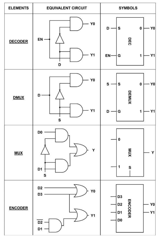
Fig. 3. Summary of logic circuits such as decoders, demultiplexers, multiplexers, and encoders. |
It's worthy to be noted that converting a decoder into a demultiplexer is as simple as connecting the data signal to the enabled input G. Additionally, the input of G is useful for establishing connections that enable the use of multiple decoders to process longer binary words.
Multiplexer
A multiplexer, often referred to as MUX, is a fundamental logic circuit that enables the selection of data from multiple inputs to be routed to a single output. Typically, it is featured with 2n data inputs, n select lines, and one output.
A 2-to-1 multiplexer, or 2 : 1 multiplexer, can be constructed as depicted in Fig. 3. The logic equation governing the 2 : 1 multiplexer is expressed as:Y = S·D0 + S·D1.
In simpler terms, when S is equal to 0, the output Y corresponds to D0, and when S equals 1, the output Y corresponds to D1.
Essentially, a 2 : 1 multiplexer operates like a commutator, which allows the switching between different inputs. Its functionality can be grasped from the schematic diagram presented in Fig. 3. By expressing the output as a function of the inputs D0 and D1, the size of the truth table for the 2 : 1 multiplexer can be reduced, making it more manageable.
Encoder
An encoder is a logic circuit which is adopted to convert input data into a specific code. Typically, it has more input variables than output variables. Take a 4 : 2 encoder as an example; it is designed to work with four inputs, with only one of them being active at a time, and produce a binary code with the adoption of two outputs. In this context, out of the potential 16 combinations of input variables, only five are valid. Fig. 3 displays the logic circuit for the resulting 4 : 2 encoder.
MATETIAL PROPERTIES OF WBG SEMICONDUCTORS
Silicon carbide (SiC) The WBG semiconductor SiC is composed of hexagonal layers of silicon (Si) and carbon (C) atoms in its crystal structure32, 33, 34. The repetition of the ABABAB pattern is capable of yielding a rhombohedral unit cell that is featured with face-centered cubic (FCC) lattices33,34. One of these lattices is comprised of Si atoms, while the others are composed of C atoms35,36. The formation of a network of covalent bonds between Si and C atoms in this configuration results in a high bond energy and a bandgap of 3.26 eV35,36. These properties make SiC a suitable material for applications that require high-temperature and power capabilities35. The crystal structure of SiC imparts distinctive properties that differentiate it from other semiconductors37,38. SiC exhibits a thermal conductivity of approximately 4.9 W cm−1 K−1. This property facilitates the dissipation of heat that arises during device operation, thereby augmenting the reliability of the device38. In addition, SiC exhibits a notable electric field strength for breakdown, denoting the upper limit of electric field intensity that the material can endure prior to experiencing breakdown39,40. SiC is capable of functioning at elevated temperatures and voltages, which surpasses other semiconductor materials like Si and GaN39.
SiC exhibits a notable characteristic of high electron mobility, denoting the velocity at which electrons can traverse the substance41,42. The attribute in question renders SiC suitable for to be employed in high-frequency applications, such as RF devices43,44. Moreover, SiC exhibits a reduced dielectric constant, which enables it to accumulate charge with lower energy consumption compared to alternative semiconductor materials45,46. SiC exhibits a Mohs hardness of approximately 9.5, making it one of the most robust materials in existence47,48. Due to its exceptional hardness and thermal conductivity, SiC is a suitable material for applications in cutting tools and high-temperature bearings47,48. The notable fracture toughness of SiC indicates its ability to endure significant mechanical loads without undergoing catastrophic failure47,48. SiC exhibits a variety of polytypes, each of them is characterized by a unique crystal lattice arrangement32,34. The polytype that is commonly utilized is 4H-SiC, which exhibits the hexagonal lattice structure as previously delineated32, 33, 34. Additional SiC polytypes are comprised of 6H-SiC, which exhibits a comparable hexagonal lattice configuration to 4H-SiC, albeit with a distinct ABABAC stacking arrangement32,35. The resulting unit cell is of rhombohedral shape, albeit it is featured with a distinct angle between the Si and C atoms.
Gallium nitride (GaN)
GaN is a kind of semiconductor material with a broad bandgap and distinctive crystal structure, which exhibits a series of material properties49, 50, 51. In GaN, wurtzite, sphalerite and rock salt are often seen to exist in the form of crystal49, 50, 51. GaN-based electrical and optoelectronic devices often exhibit the wurtzite crystal structure52,53. The arrangement of Ga and N atoms in alternating layers make the structure of the material exhibit a hexagonal lattice pattern. The tetrahedral arrangement of the structure is determined by the four nitrogen atoms surrounding each gallium atom and the four gallium atoms surrounding each nitrogen atom52. Significant characteristics of the wurtzite crystal structure, such as increased electron mobility, make it a viable substitute for electronic devices that need high-speed performance54,55. It also exhibits a high level of thermal conductivity, making it a good choice for applications involving high temperatures56,57. Compared to the wurtzite structure, the zinc blende type of the GaN crystal structure is comparatively uncommon58,59, however, it is endowed with special qualities which shows advantages for applications in some scenarios56,58. The chemical exhibits a cubic lattice structure with the same number of gallium and nitrogen atoms with its crystal structure. According to the structure, there exist four N atoms around each Ga atom and four Ga atoms surrounding each N atom. When compared to the wurtzite structure, the zinc blende version of the GaN crystal structure exhibits lower bandgap energy, making it a viable alternative for optoelectronic applications.
GaN exhibits distinct crystal structures, and a variety of doping methods could be adopted to change the characteristics of the material. p-Type GaN may be resulted from the incorporation of magnesium (Mg) whereas n-type GaN from the incorporation of silicon (Si)60, 61, 62. The electrical and optical properties of GaN may be changed by doping with other elements, such as oxygen (O) and zinc (Zn)60, 61, 62. As was discussed in the previous discourse, the crystal structures of GaN could exert a considerable influence on both its material qualities and appropriateness for a variety of applications. The wurtzite crystal structure is often used in GaN-based electrical and optoelectronic devices. On the other hand, the zinc blende and rocksalt structures are endowed with distinctive qualities that make them suited for certain applications. With the continuous advancement of researches and development in the fields of electronics and optoelectronics, GaN is predicted to play a larger role in high-performance equipment.
Zinc oxide (ZnO)
ZnO, is a versatile semiconductor material with wurtzite as its primary crystal structure and exhibits a broad bandgap. The crystal structure of ZnO has a big impact on how it determines its material qualities and appropriateness for a variety of applications63, 64, 65. The crystal structure of wurtzite is a hexagonal closely packed lattice composed of two interpenetrating triangular sublattices that interpenetrate one another63, 64, 65. The Zn ions in ZnO can be shown to be located in one of the sublattices, whereas the O ions are found to exist in the other sublattice. Each Zn ion is coordinated by four O ions in a tetrahedral arrangement, while each O ion is coordinated by three Zn ions in a trigonometric configuration. With the lattice parameters of a = b = 3.25 and c = 5.20 and an inter-axis angle of 120° between the c-axis and the a-axis, ZnO exhibits a crystal structure66, 67, 68. The asymmetrical arrangement of Zn and O ions is thought to be responsible for the surface charge that first appeared along the c-axis and the polar character of the wurtzite crystal structure66, 67, 68. A variety of flaws may exist in the crystal structure of ZnO, including point defects, extended defects, and surface defects, which may affect the properties of the material69,70. In ZnO, oxygen vacancies are a common point defect that lead to the development of shallow donors and n-type conductivity69,70. Zinc interstitials are a particular kind of point defect that might potentially lead to p-type conductivity in ZnO71,72. Extended defects, including dislocations, stacking faults, and grain boundaries, may affect the properties of ZnO materials71,72. The bandgap may be created by these flaws with localized states. Surface flaws such as steps, terraces, and interface flaws, may introduce surface states and exert an impact on the electrical and optical characteristics of ZnO.
The polarity of wurtzite crystal structure allows for the generation of an electric charge in reaction to mechanical stress, ZnO exhibits the piezoelectric phenomenon73, 74, 75. Due to the piezoelectric properties, ZnO is suitable for application in a variety of sensing and actuation situations73, 74, 75. The phenomena of surface charge generation at the ZnO/other material contact, which is caused by ZnO's polarity, could exert a substantial effect on the electrical properties of the material73. Due to its large bandgap of around 3.37 eV and outstanding transparency in the visible spectrum, ZnO exhibits excellent optical properties76, 77, 78. For application in transparent conductive electrodes for photovoltaic and optoelectronic devices, ZnO is a suitable alternative due to its high degree of transparency76, 77, 78. Al, Ga, In, and Li are some of the dopants that may be used to manipulate the bandgap of ZnO. Significant excitonic effects are produced by the tight coupling between the electron and hole in ZnO79, 80, 81. At ambient temperature, this causes the formation of excitons with binding energies reaching as high as 60 meV79, 80, 81. ZnO material properties and suitability for a variety of applications are strongly influenced by its wurtzite crystal structure. The crystal structure of the material could exert an impact on both its piezoelectricity and electrical characteristics. The material qualities of ZnO may be affected by flaws in its crystal structure, highlighting the need of controlling growth and processing settings to reduce the likelihood of such flaws. ZnO is a very advantageous chemical which is widely applied in the fields of electronics, optoelectronics, and photonic equipment owing to its remarkable optical properties, broad bandgap, and piezoelectric properties.
Indium oxide (In2O3)
Rhombohedral crystal structure is a characteristic of the semiconductor In2O3. The crystal structure of In2O3 may be described as a spinel-type structure, whereby indium atoms occupy tetrahedral and octahedral positions in the interstitial gaps while oxygen atoms form a cubic, tightly packed structure82, 83, 84. Thirty oxygen atoms and ten indium atoms make up the rhombohedral unit cell of In2O385, 86, 87. Six octahedral sites and four tetrahedral sites each contain one indium atom. With a face-centered cubic structure and a dense packing of oxygen atoms, the arrangement of oxygen atoms is distinctive85, 86, 87. Notably, there is an open place that should be inhabited by an oxygen atom. When indium atoms are positioned inside the interstitial spaces of oxygen atoms, octahedral and tetrahedral structures are created. The coordination environment for each indium atom in the octahedral sites consists of six oxygen atoms, while the coordination environment for each indium atom in the tetrahedral sites is composed of four oxygen atoms. The crystal structure of In2O3 may be regarded as an octahedral-octahedral tiled rhombohedral Bravais lattice. The remarkable stability and symmetry of the In2O3 crystal structure make it an attractive material with a variety of applications88, 89, 90. The distinguishing properties of In2O3, including its high electron mobility, outstanding transparency in the visible and near-infrared spectra, and a bandgap of around 3.7 eV, are mainly ascribed to its rhombohedral crystal structure88, 89, 90.
The remarkable symmetry in the crystal structure of In2O3 also contributes to its remarkable electrical and magnetic capabilities91, 92, 93. The crystal structure exhibits a large number of surface terminations, which might lead to the formation of surface states and changes in the electrical properties of the substances91, 92, 93. The arrangement of the material's magnetic spins is also non-collinear, indicating that the spin orientations of the neighboring indium atoms are neither parallel nor antiparallel to one another. In2O3, a compelling material for many applications in the fields of electronics, optoelectronics, and magnetic materials, is characterized by a high degree of stability and symmetry and exhibits notable electrical and magnetic characteristics91, 92, 93. In2O3 thin films may be deposited with the adoption of a variety of methods to produce amorphous indium oxide (a-In2O3)94, 95, 96, including sputtering, chemical vapor deposition, and atomic layer deposition. The amorphous phase of In2O3 is distinguished from the crystalline form by the lack of a clearly defined, periodic atomic arrangement and the presence of a disordered network of interconnecting atoms94, 95, 96. In2O3 exhibits a high electrical conductivity, which highlights a key characteristic and makes it a good candidate for use in transparent conducting oxide (TCO) applications97, 98, 99. Due to their outstanding transparency in the visible and near-infrared spectrums and low electrical resistance, transparent conductive oxides (TCOs) are applied in a variety of areas, including solar cells, flat panel displays, and touch screens97, 98, 99. A notable property that is equivalent to that of crystalline In2O3 is the high electron mobility of In2O3. Due to its high conductivity and fast electron mobility, the material In2O3 is thought to be suitable for high-speed electronics applications100, 101, 102. In2O3 in its amorphous form shows great resistance to chemical reactions and thermal degradation, making it a practical choice for use in harsh environments and high-temperature situations103, 104, 105. Furthermore, owing to the enhanced reactivity to reducing gases, such as but not limited to hydrogen and carbon monoxide, a-In2O3 has been recognized as a potentially advantageous choice for gas sensing applications.
IGZO
The compound semiconductor IGZO, which is comprised of indium, gallium and zinc, has been the subject of extensive researches owing to its remarkable electrical characteristics and transparency106, 107, 108. The crystallographic configuration of IGZO is distinguished by a considerable level of intricacy, where the crystal lattice contains three distinct elements with unique positional occupancy. The objective of this study is to conduct a thorough examination of the crystal structure of IGZO106, 107, 108. The chemical compound InGaZnO4, commonly referred to as IGZO, is classified as a quaternary compound semiconductor109, 110, 111. The crystal structure of IGZO is categorized within the spinel family of structures, which is distinguished by the arrangement of tetrahedral and octahedral sites in an array109, 110, 111. The intricate nature of the spinel crystal structure can be attributed to the coexistence of metallic atoms in both the tetrahedral and octahedral positions within its framework. The IGZO crystal structure exhibits a cubic lattice and is associated with a Fd-3m space group112, 113, 114. The IGZO substance displays a lattice constant of approximately 8.08 and a lattice parameter ratio of c/a = 1.628 112, 113, 114. The unit cell of the crystal structure is composed of 32 atoms that are dispersed among 16 tetrahedral sites and 8 octahedral sites112, 113, 114.
The crystal structure of IGZO is distinguished by the presence of In3+ cations occupying octahedral sites, while Ga3+ and Zn2+ cations occupy tetrahedral sites115, 116, 117. The cations with a positive charge are surrounded by the negatively charged anionic oxygen species. These oxygen species are situated in both tetrahedral and octahedral coordination environments115, 116, 117. The tetrahedral coordination of oxygen atoms requires the presence of two cations, while six cations are needed for the octahedral coordination of oxygen atoms115, 116, 117. The crystal structure of IGZO has been extensively studied with the adoption of various experimental techniques such as X-ray diffraction, transmission electron microscopy, and Raman spectroscopy118, 119, 120, 121, 122. The implementation of these methodologies has contributed to noteworthy discoveries pertaining to the crystallographic configuration and properties of IGZO118, 119, 120, 121, 122. Moreover, the utilization of these methods has enabled the augmentation of their effectiveness for various implementations, including but not limited to TFTs, photovoltaic cells and electroluminescent devices.
Gallium oxide (Ga2O3)
A semiconductor with a broad bandgap and a high breakdown voltage is referred to as Ga2O3123, 124, 125. It is a very desirable material for a wide variety of electrical and optoelectronic applications owing to its unique mix of characteristics. The crystalline configuration of Ga2O3 bears striking similarities to that of the aluminum oxide. Ga2O3 exhibits five different polytypes such as α, β, γ, δ, and ε126, 127, 128. Ga2O3's α-polymorph is a hexagonal crystal structure, and its space group is P63mc129, 130, 131. In comparison to the α-phase, the β-phase displays a less dense arrangement that is marked by a smaller number of oxygen atoms in the unit cell and a higher lattice constant along the c-axis132,133. At lower temperatures, the stability of β-phase is noticeably less stable than that of the α-phase. For the development of the β-phase, a variety of techniques may be used, such as sputtering, pulsed laser deposition (PLD), and atomic layer deposition (ALD)134,135.
The space group Ia-3 distinguishes the cubic crystal structure of the γ-polymorph of Ga2O3. As the least common one among the five identified varieties, the polytype shows stability at high temperatures and pressures136,137. The crystal structure of the polymorph is rhombohedral in nature and has the space group R3c. The polymorph, on the other hand, exhibits a tetragonal crystal structure and possesses the space group P42/nmc136,137.
Diamond
The three-dimensional arrangement of carbon atoms in the crystal structure of a diamond is distinguished by a FCC lattice, which is resulted from the covalent bonding138, 139, 140. This unique arrangement makes diamond a notable semiconductor. The tetrahedral bonding of carbon atoms to four neighboring carbon atoms leads to a sturdy and rigid structure that displays remarkable resistance to deformation138, 139, 140. The diamond lattice displays a high level of symmetry, which is described by a space group denoted as Fd-3m and a lattice constant of 0.356 nm141, 142, 143. Diamond exhibits the broad bandgap of 5.5 eV and shows exceptional electrical insulation properties, rendering it a material of significant importance144,145. The optical transparency of diamond across a wide range of wavelengths makes it a favorable material for multiple applications, including the manufacturing of optical windows and lenses, and as a substrate for the growth of other semiconductors146,147.
In addition to its intrinsic properties, the diamond crystal structure can be modified via the technique of impurity doping, whereby elements such as boron or nitrogen are introduced during the growth stage148-150. The process described above could potentially result in the creation of either p-type or n-type diamonds, which in turn facilitates the development of diamond-based electronic devices148, 149, 150. Diamond demonstrates remarkable thermal conductivity characteristics, exceeding those of all the other known materials. At standard room temperature, its thermal conductivity value is estimated to be around 2200 W m−1 K−1 151-153. Diamond has been identified as a material with high potential for thermal management applications, such as serving as substrates for high-power electronic devices and heat sinks151-153.
SINGLE CRYSTALLINE WBG SEMICONDUCTOR-BASED DEVICES AND CIRCUITS
SiC Over the last 20 years, SiC has been the subject of researches for its prospective application in logic circuits154. Compared to traditional silicon-based logic circuits, SiC-based logic circuits are endowed with several benefits such as improved radiation tolerance, increased operational temperatures, and quicker switching speeds5,155, 156, 157. SiC-based logic circuits possess inherent advantages that make them suitable for application in various fields, including but not limited to aerospace, automotive and military5,155.
Singh et al.154 have successfully produced circuits adopting the emitter-coupled logic (ECL) technology. The optimized design for silicon carbide bipolar junction transistors (SiC BJT) has been presented by the authors, who have also demonstrated their application in ECL circuits. The circuits have been designed to function at elevated temperatures and high speeds, exhibiting noise margins of approximately 0.9 V at room temperature and propagation delays of approximately 2.8 ns. The research findings suggest that the ECL ICs implemented in SiC demonstrate consistent properties even under fluctuating power supply voltages and high temperatures, thereby demonstrating their viability for employment in compact logic systems.
Lanni et al.158 documented the results of their study, which involved the examination of Integrated Digital Circuits that were produced through the utilization of a bipolar SiC technology. The circuits were found to be capable of functioning at temperatures reaching 600 °C. The consistent noise margins of OR-NOR gates are observed to be around 1 V. Additionally, when powered by a −15 V supply voltage within the temperature range of 27 - 600 °C, these gates exhibit an increasing delay-power consumption product within the range of 100 - 200 nJ. The oscillation frequency of an 11-stage ring oscillator has been reported to be approximately 1 MHz within a specific temperature range. The operational temperature limit is around 600 °C for SiC-based circuits. Logic gates and oscillator circuits were demonstrated over a temperature range spanning from 27 to 600 °C.
Encouraging outcomes have been obtained for NMOS logic gates based on 4H-SiC by Huu et al.160 Typically, NMOS logic gates for high temperature applications are fabricated with the adoption of enhancement mode SiC transistors. The characterization of logic gates is performed over a temperature range spanning from 25 to 500 °C. The research showcases the functionality of stable gates over a period of more than 200 h while being subjected to a temperature of 400 °C in an atmosphere consisting of air. At the temperature of 400 °C, the height of the tunneling barrier for electrons experiences a reduction, resulting in an effective height of 2 eV. The lifetime extrapolated from constant voltage stress to breakdown measurements surpasses 105 h at the given temperature. This phenomenon is noted in a standard logic gate that functions at a field intensity of 2 MV cm−1.
Aissa et al.159 conducted researches focusing on the ambipolar functionality exhibited by thin film field-effect transistors with back-gate configuration (Fig. 4). The transistors are constructed through a drop casting process utilizing hybrid networks of n-type SiC and p-type single-walled carbon nanotubes. The research produced noteworthy outcomes, such as a ratio of 105 for on and off states and a subthreshold swing of below 165 mV/decade (Fig. 4b). The devices that were stable in air exhibited ambipolar operational characteristics that persisted for over two months in an ambient environment. This marks a significant progress towards attaining dependable functionality in electronic systems at the nanoscale.
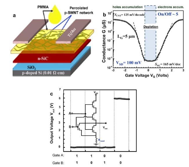
Fig. 4. a, Schematic illustration and b, Electrical characteristics of SiC-based bottom-gate device. c, Output characteristics of NOR gate circuit. Reprinted with permission from ref.159. © 2012 American Institute of Physics. |
Lee et al.161 reported the progress of creating monolithic bipolar TTL integrated circuits with the adoption of 4H-SiC material. The study of voltage-transfer characteristics (VTCs) of SiC TTL inverters, operated at a voltage of VCC = 15 V, reveals NMH and NML around 1.5 and 3.9 V, respectively. The preservation of noise margins remains consistent over a broad spectrum of temperatures, ranging from standard room temperature to temperatures surpassing 300 °C. The study indicates that an increase in temperature above 300 °C leads to a minor reduction in propagation delay. The results exhibit that SiC-based logic circuits is promising to be utilized in high-temperature environments; however, additional investigation is required to establish the sustained reliability of the technology.
Lanni et al.162 have effectively fabricated ECL ICs utilizing 4H-SiC, and have demonstrated their successful operation at elevated temperatures of up to 300 °C. The OR-NOR gate that was reported has demonstrated consistent noise margins at around 1 V across a temperature spectrum ranging from 27 to 300 °C. The resonant oscillator that was artificially created has been observed to demonstrate a consistent oscillation frequency of roughly 2 MHz throughout all temperature variations. The OR-NOR gate could experience a decrease in both circuit area and propagation delay through the process of circuit design optimization. The reported technology of integrated circuits shows potential as a viable option for applications with the requirement of elevated temperatures.
Philip and colleagues163eported their research findings on the brief exhibitions of integrated circuits (ICs) that employed packaged 4H-SiC JFETs. The expanded temperature range is anticipated to aid in the process of temperature acceleration testing and certification of integrated circuits that are engineered for extended operation in environments with ambient temperatures of around 500 °C. According to the research results, the utilization of BJTs and an integrated bipolar OR/NOR gate has demonstrated successful operation in 4H-SiC at elevated temperature of up to 500 °C. Enhancements in device performance and the integration of a temperature compensation network contributed to the increased stability of noise margins (NMs). The stability of NMs is observed to be around 1 V across a temperature range of 25 to 500 °C, albeit with a minor decline at lower temperatures.
Despite these advantages, several challenges still remain to be addressed before achieving extensive adoption of logic circuits based on SiC. The limited availability of high-quality SiC substrates present a significant obstacle. One of the challenges faced in incorporating SiC components into the existing electronic frameworks is the lack of advanced manufacturing techniques for SiC-based logic circuits. This presents an additional obstacle to the assimilation of SiC-based components. In summary, SiC-based logic circuits offer several advantages over conventional silicon-based circuits, including improved operational speeds, higher operating temperatures, and better radiation resistance. Despite the challenges associated with SiC-based logic circuits, significant progress has been made in recent years in the development of SiC-based devices and integration techniques. Logic circuits based on SiC exhibit the potential to enable a new generation of electronic systems that are characterized by superior performance and reliability and can cater to a wide range of applications.
GaN logic circuits
The source, drain, and gate terminals make up the tripartite arrangement of GaN high electron mobility transistor (HEMT)164,165. The gate voltage controls both the modulation of electron charges and the current transfer164,165. The outstanding characteristics of HEMTs in terms of improved electron mobility, quick switching, and increased breakdown voltage have been shown164,165. A thin insulating layer is included between the gate and the channel in the GaN metal-insulator-semiconductor high electron mobility transistors (MIS-HEMTs), which are an altered form of the standard GaN HEMT166-168. The decrease in gate leakage current and increase in gate capacitance are both the reasons accounting for the improved device performance166-168. A junction between a metal and a semiconductor makes up the GaN Schottky barrier diode (SBD), a two-terminal semiconductor device169-171. Due to its higher Schottky barrier height and lower reverse leakage current than conventional silicon-based diodes, GaN SBDs exhibit superior functionality169-171.
A semiconductor is with two separate layers of GaN, one of which is p-type and the other n-type, the GaN p-n diode is distinguished by the presence of two terminals169. GaN p-n diodes have been proven to offer the potential for usage in high-power and high-frequency applications169-171. The use of GaN HEMT in logic circuits is acceptable due to its beneficial properties, which include high-frequency and high-power capabilities6,172,173. According to researches, GaN HEMTs may operate at clock speed of up to 1 GHz, making them ideal for high-speed digital circuits169,173. Additionally, earlier studies have shown that GaN HEMTs show amazing logic switching properties, such as increased amplification and reduced switching latency. GaN HEMTs exhibit qualities that make them suitable for high-speed digital circuits6,172,173.
Monolithic integrated E/D mode MIS-HEMTs were adopted by Zhu et al.174 to create logic gate circuits for the NAND, NOR, AND, and OR operations. Subsequently, the same wafer was employed for the implementation of the DFF arrangement based on NOR and NAND. The highest voltage that can be applied to the logic circuits is 9 V, and the logical truth table was found to match the empirical data, making logical judgment a success. The current discovery demonstrates the use of MIS-HEMT in creating high-frequency logic circuits with high input voltage.
In a work conducted by Chowdhury et al.175, they showed how to build an inverter complementary logic circuit on a GaN-on-Si substrate without using regrowth technology. In the enhancement mode, electron channel FET functionality was shown. The use of technology to create complementary logic inverters resulted in 27 V/V voltage gain, as well as exceptional performance up to the operating temperatures of 300 °C, which indicates the potential of this technology for incorporation in electronic applications that require low power consumption and high-performance.
WBG technology has been successfully adopted by Chenhao et al.8 to produce a complementary metal-oxide-semiconductor (CMOS) building block. The aforementioned construction block showed operational effectiveness even at temperatures higher than 350 °C. Diamond and GaN, which are two material systems with large bandgaps and renowned for their outstanding ability to withstand high temperatures, were employed in the development of the CMOS technology. Discrete semiconductor materials were used to create PMOS and NMOS devices. The diamond field-effect transistor used by the PMOS contains a hole channel, which was made possible with the adoption of a hydrogen-terminated method. In contrast, the NMOS was made up of a GaN high electron mobility transistor (GaN HEMT) electron channel.
Zheng et al.176 conducted researches on the development of a ring oscillator using GaN technology. The logic circuits were used in the fabrication of the oscillator, which was done on a standard p-GaN gate power HEMT platform. The study demonstrates the viability of integrating monolithic GaN CL gates across a number of stages. The extraordinary energy efficiency of this specific design in digital circuits raised the possibility that CL circuits might be used as peripheral circuits. The operations displayed strict rail-to-rail functionality and significantly lower static power consumption.
Cai et al.177 published their results concerning the fabrication and evaluation of oscillators and inverters using GaN technology. An important benefit of plasma treatment of E-mode HEMTs is the reduction of gate current in both the reverse bias and the forward bias regions. Findings on a newly created multi-stage ring oscillator that was made using 1-μm gate technology were presented in the study article.
By adopting fluoride-based plasma treatment procedures, Wang et al.178 developed a novel planar manufacturing technology that integrates mode AlGaN/GaN HEMTs. The oscillator has been shown to operate well at a higher supply voltage of 3.5 V. The use of CF4 plasma therapy is a two-pronged process that seeks to accomplish two distinct goals. This method has two benefits: firstly, it encourages the separation of active devices; secondly, it makes it possible to adjust the threshold voltage during the production of E-mode HEMTs. The planar technique is used to create E/D-mode HEMTs on a single chip. This procedure results in the creation of a 17-stage ring oscillator and a DCFL inverter. With no discernible variations in device isolation, HEMTs which is made with the adoption of planar processing exhibit similar DC and RF properties to those made using traditional mesa etching. At a 3.3 V supply voltage, the E/D-mode inverter exhibits a 2.85 V output swing along with logic low and high noise margins of 0.34 and 1.47 V, respectively. The devices demonstrate minor changes in their DC and RF properties after experiencing 44-h thermal stress at 350 °C, confirming the extraordinary thermal durability of the planar method. The ring oscillator, once created, exhibits an oscillating frequency of 159 MHz when driven by 4.5 V.
In a work conducted by Chen et al.179, they successfully built a GaN inverter that integrated HEMTs on a Si substrate. The epitaxial layer thickness and doping method were optimized to provide an NMH and NML of around 1.47 V and 0.98 V, respectively. In a ring oscillator, the propagation delay was measured to be 1.67 ns according to the conclusions of the study, the development of GaN power modules may greatly benefit from the use of complementary FET technology.
However, there exist several difficulties in using GaN HEMTs in logic circuits. The increased expense of GaN HEMT technology in comparison to conventional silicon-based technology is one key obstacle. One notable difficulty is the absence of standardization in GaN HEMT device configuration, which might cause compatibility problems with other parts and systems. In conclusion, the adoption of GaN HEMT technology shows substantial benefits over traditional silicon-based technology, particularly in terms of its capacity to carry out high-frequency, high-power, and high-temperature activities. GaN HEMTs are a good alternative for use in high-speed digital logic circuits like digital signal processors, microcontrollers, and FPGAs due to their beneficial characteristics. GaN HEMTs hold great promise for the approaching era of high-speed and high-power electronic applications, despite the challenges associated with their implementation in logic circuits. The advantages they provide exceed the costs involved.
Ga2O3
The MISFET Ga2O3 transistor architecture has attracted the greatest research interest181,184,185. In this kind of transistor, the Ga2O3 channel is separated from the metal gate by a thin insulating layer. The transistor can be switched between its on and off states more easily due to the gate voltage's modulation of the carrier concentration in the channel. Ga2O3 MISFETs with extraordinary performance characteristics, such as significant drain current densities, high on/off ratios, and significant breakdown voltages, have been successfully fabricated according to several research projects181,184,185.
A Schottky connection exists between a metal gate and the Ga2O3 channel in SBFETs187, 188, 189. Due to the absence of an insulating layer in the gate stack, they have been shown to exhibit faster switching speeds than MISFETs. Compared to MISFETs, SBFETs often exhibit worse on/off ratios and higher gate leakage currents181,187-189. Ga2O3-based CMOS integrated circuit development is a young area, with significant advancements only made in the last few years. Ga2O3 makes an appealing option for high-end power devices and electronics that run at high temperatures owing to its unique properties. By employing a van der Waals heterojunction, Kim et al.183 develop an E-mode quasi-2D—Ga2O3 FET with a distinctive graphene gate structure (Fig. 5). The authors realized monolithic integration of β-Ga2O3 devices to create a logic circuit that is effective in terms of its size. β-Ga2O3 MESFETs in the E- and D-modes were found to exhibit good electrical properties.
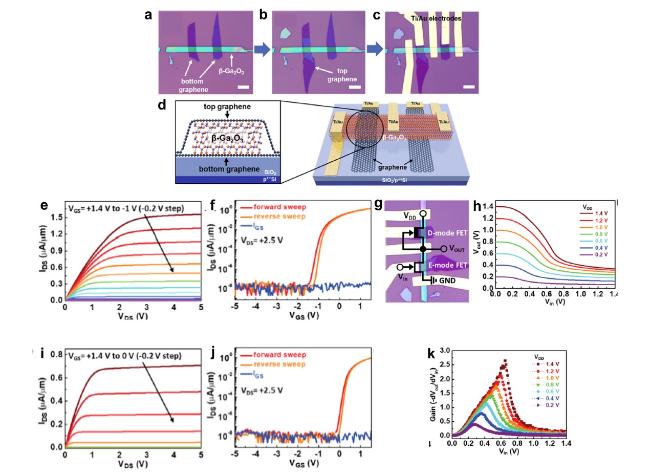
Fig. 5. a-c, Optical micrograph and d, schematic illustration of β-Ga2O3 MESFET device. Electrical characteristics of e-f, single-gate and g-h, dual-gate MESFET device. i-k, Electrical characteristics of β-Ga2O3 NMOS logic inverter circuit. Reprinted with permission from ref.183. © 2020 American Chemical Society. |
The monolithic integration of a quasi-2D FET with a UWBG channel layer enables a variety of intelligent and resilient power (nano) electronics applications. Inverter circuits and flexible β-Ga2O3 TFTs may both be made via solution processing, according to researches performed by Bhalerao and colleagues190. High-k Al2O3, which was formed via a room-temperature anodization procedure, served as the gate dielectric in this work. The performance characteristics of Ga2O3 TFTs are noteworthy. In particular, the observed extracted electron mobility is 2.74 cm2V−1s−1, the working voltage is 3 V, and the VTH is 0.61 V. Additionally, the subthreshold swing (SS) is 0.5 V/dec and the ION/IOFF is 10. The transconductance is 64.8 S, and the hysteresis is 0.1 V. Chen and his associates191 have proposed and shown the viability of a solar-blind photo-memory array that makes use of β-Ga2O3. This array can execute math, logic, and optoelectronic memory operations. The results show that the device performs as an n-type field effect transistor, which is distinguished by a high ION/IOFF ratio of up to 106. These numbers are significant since they are among the highest yet recorded for photodetectors made of β-Ga2O3. Utilizing the trapping and detrapping operations of the holes in β-Ga2O3 allows for multilevel data storage. In addition, the photomemory array may be used to store photos that are resistant to sun radiation. The results show that β-Ga2O3 has intriguing applications in cutting-edge data storage, computing, and communication technologies. Recently, Khandelwal et al.186 reported an NMOS inverter using β-Ga2O3 devices (Fig. 6). The E-mode devices exhibited a current ratio and VTH of approximately 105 and 3 V, respectively. In addition, the fabrication of depletion-load NMOS inverter integrated circuits involved the monolithic integration of D- and E-mode transistors on a single substrate. The NMOS integrated circuits exhibited the operation of inverter logic and a voltage gain of 2.5 at a VDD of 9 V, which is like the performance of recent inverters based on wide-bandgap semiconductors such as GaN192.
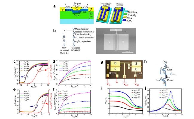
Fig. 6. a, Schematic illustration, b, Fabrication process and b-right, SEM image of β-Ga2O3 TFT device. c-f, Transfer and output characteristics of β-Ga2O3 TFT device. g, Optical micrograph, h, Circuit diagram, and i-j, Electrical characteristics of logic inverter circuit. Reprinted with permission from ref.186. © 2023 American Institute of Physics. |
In conclusion, it can be said that applications which require high-power and high-temperature tolerance show tremendous promise for CMOS integrated circuits based on β-Ga2O3. However, there are several significant challenges that must be overcome, such as the lack of a suitable high-k gate dielectric material and the high concentration of interface states. In order to increase the reliability and efficiency of MOSFETs based on β-Ga2O3, it is advised that future research efforts should be focused on the development of suitable gate dielectric materials and surface treatments.
Diamond
The diamond MISFET is a promising configuration for diamond-based transistors193, 194, 195. The electronic device is composed of a channel made of diamond, a gate made of metal, and a dielectric layer for the gate. The gate dielectric can be composed of various materials, such as SiO2, Si3N4, or Al2O3. The diamond MISFET has been observed to possess highly advantageous electrical characteristics, including exceptional carrier mobility, negligible leakage current, and significant transconductance. The production of high-quality gate dielectric on diamond has posed a challenge to the effective realization of diamond MISFETs in practical applications193, 194, 195. Studies have been carried out pertaining to BJTs fabricated from diamond material4,196,197. The BJTs are constructed using a p-type diamond base, an n-type diamond emitter, and a collector made of metal4,196,197. The diamond BJT has demonstrated remarkable features including heightened current amplification, augmented breakdown voltage, and improved thermal durability. The efficiency of diamond BJTs has been hindered due to limitations in achieving superior diamond p-n junctions and higher doping levels in diamond4,196,197.
Considerable investigation has been carried out on Schottky diodes made of diamond, which consist of a metal-semiconductor interface formed between a metal contact and a diamond material198, 199, 200. Diamond Schottky diodes have demonstrated remarkable properties, including decreased leakage current, increased breakdown voltage, and the capacity to function at elevated temperatures198, 199, 200. The application of diamond Schottky diodes in practical settings has been limited due to the challenge of producing high-quality metal contacts on diamond material198, 199, 200.
Liu et al.201 conducted the production and analysis of NOR logic circuits composed of hydrogenated diamond. The study demonstrated the manufacturing process and the significance of annealing in relation to the electrical properties of the NOR logic circuit. The logical characteristics of NOR circuits displayed distinct behavior under both 25 and 300 °C annealing conditions (Fig. 7). In contrast, in the given scenario, when the input voltages were measured at 0 V and categorized as ““low” signals, the resultant output voltage demonstrated a response of −10 V and a ““high” signal. The degradation of H-diamond MOSFETs may be the reason accounting for the damage observed in the NOR logical characteristics following annealing at 400 °C. The utilization of a diamond-based MISFET with a load resistor was demonstrated by Liu et al.202 The gate's insulator displayed a bilayer structure comprising of a LaAlO3 layer that was sputter-deposited and a thin buffer layer of Al2O3 that was deposited through atomic layer deposition. The study has successfully achieved the maximum source-drain current (40.7 mA mm−1), extrinsic transconductance (13.2 ± 0.1 mS mm−1), and threshold voltage (−3.1 ± 0.1 V) of the MISFET. The empirical findings pertaining to the conduct of logic inverters suggest a distinct pattern of inversion, specifically that of a NOT-gate. The gain of the logic inverter exhibits a proportional increase with increasing load resistance, with values ranging from 5.6 to the maximum of 19.4 V.
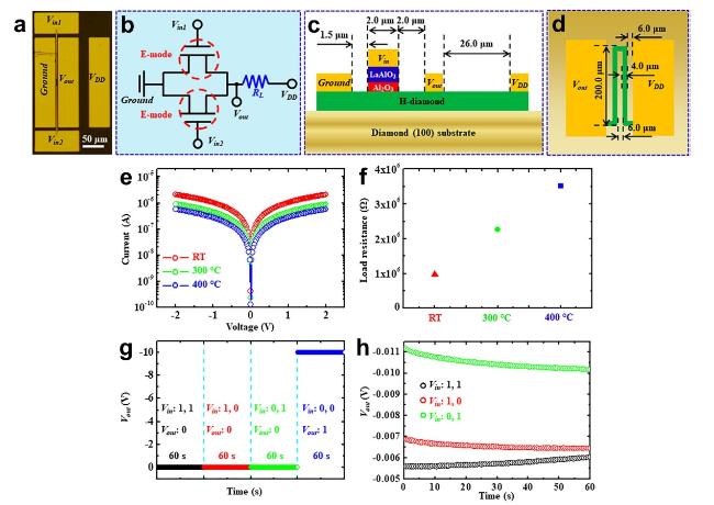
Fig. 7. a, Optical micrograph, b, Circuit diagram and c-d, Schematic illustration of diamond-based NOR logic circuit. e- f, I-V characteristics of diamond TFT device. g-h, Electrical characteristics of NOR logic circuit. Reprinted with permission from ref.201. © 2018 American Institute of Physics. |
Liu et al.203 conducted a study in which bilayer dielectric materials were deposited onto the diamond channel layer. The application of thin ALD-Al2O3 films as buffer layers on H-diamond is a prevalent technique employed to alleviate the plasma discharge impact and diminish the leakage current density (J) of SD-TiO2 and ALD-TiO2. This study focused on the examination of the electrical characteristics exhibited by transistors and logic inverters constructed through the utilization of TiO2/Al2O3/H-diamond (Fig. 8).
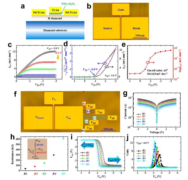
Fig. 8. a, Schematic illustration, b, Optical micrograph, and c-e, Electrical characteristics of diamond-based MOSFET device. f, Optical micrograph of diamond logic inverter connected to different load resistors. g-j, Electrical characteristics of diamond logic inverter circuit. Reprinted with permission from ref.203. © 2017 American Institute of Physics. |
Holmes et al.204 fabricated the MOSFETs with the adoption of homoepitaxial-diamond-thin films. The chosen specimens underwent current-voltage characteristic measurements over a temperature spectrum ranging from 25 to 500 °C. Advancements in the techniques of diamond growth and device fabrication resulted in an enhancement of the uniformity of transconductance and drain-to-source current across a particular sample. The research entailed the characterization of a common source amplifier circuit that employed a diamond MOSFET. The utilized input signals spanned a frequency range of 20 Hz to 1 MHz, and the circuit exhibited a direct current gain of 5 when subjected to a temperature of 250 °C. The present study showcases the operational efficacy of a set of diamond MOSFETs that were configured as NAND and NOR digital logic gates, at an elevated temperature of 400 °C. Liu et al.205 employed a selective growth technique utilizing a noble metal (Ti/Ru) mask to fabricate diamond Schottky diodes. At a temperature of 633 K, the Schottky device demonstrated a substantial rectification ratio of 109, indicating a promising performance at elevated temperatures. Various methodologies have been utilized in the derivation of Schottky diode parameters, and their appropriateness has been assessed through comparative scrutiny. The reliable operation of a logic AND circuit at 633 K was achieved through the implementation of Schottky diodes. The discovery implies that the diodes in question exhibit significant potential for being incorporated into microprocessors designed to function in elevated temperature settings.
Ghosh et al.206 reported the achievement of vacuum microelectronic OR gate logic through the utilization of nanodiamond lateral diode structures, which were successfully fabricated and characterized. The diodes exhibited variation in the number of emitters they possessed, namely 125, 325, 2340 and 9360 (Fig. 9). The distance between the anode and cathode for both sets was approximately 3.5 μm. The fabricated lateral emitters were subjected to characterization to investigate the scaling effect of different structures on the forward emission current. Following this, a set of identical diodes were incorporated into a circuit that utilizes diode-resistor logic to execute the logical OR function, utilizing a square wave as the input signal. The current scaling trend was observed in the current study, wherein the current of 1 A was recorded at different voltage levels, namely 18, 15, 7 and 2.2 V, for emitter structures comprising 125, 325, 2340, and 9360 fingers, respectively. This trend is found to have a significant influence on the logic OR response. The prospect of utilizing nanodiamond vacuum logic gates in challenging environments holds great promise. Recent developments in diamond CMOS logic circuits have demonstrated the potential of diamond as a viable material for the next generation of electronics. Based on the reported results, it can be inferred that diamond has achieved noteworthy advancements in cutting-edge technology. Despite the significant challenges that remain in achieving high-quality p-type diamond and improving hole mobility in diamond, the promising results achieved thus far suggest that diamond CMOS circuits may show significant advantages over silicon CMOS circuits in terms of performance, reliability and scalability.
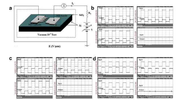
Fig. 9. a, Schematic illustration of diamond based diode device. Output characteristics of OR gate designed by diode having b, 125, c, 325, and d, 9360-finges. Reprinted with permission from ref.206. © 2012 Elsevier BV. |
THIN FILM WBG SEMICONDUCTOR-BASED DEVICES AND LOGIC CIRCUITS
ZnO Comparing traditional silicon-based technology to ZnO, various benefits may be seen. Its increased electron mobility, which enables faster switching rates and less energy use, is the main advantage207-209. Since ZnO has a larger bandgap than silicon, it is more resistant to breakdown and can operate at higher temperatures. ZnO is a strong contender for use in optoelectronics since it also shows transparency207-209. Low-temperature deposition methods, such as sputtering or atomic layer deposition, are often used to create TFTs210-212. By adopting these approaches, thin layers of ZnO may be formed on a variety of substrates, including flexible polymers and glass210-212. Top-gate and bottom-gate transistors are the two categories under which TFTs fall. The gate electrode for top-gate TFTs is deposited on the surface of ZnO film. On the other hand, bottom-gate TFTs call for the deposition of the gate electrode on the substrate, followed by the deposition of the ZnO film on top of the gate. Flat panel displays and sensors are only two examples of the many applications for TFTs210-212. ZnO logic circuits, which include inverters, NAND gates, NOR gates, and multiplexers, have been shown to operate by several research teams. These circuits have been produced using a variety of manufacturing processes, including chemical vapor deposition, pulsed laser deposition, and sputtering. One significant benefit that promotes the development of stretchable and wearable electronics is ZnO logic circuits' compatibility with flexible substrates.
For instance, the authors Kang et al.213 described building logic circuits using ZnO nanowires. Multiple layers of FETs on plastic substrates were vertically integrated to create the circuits. Through thermal chemical vapor deposition, ZnO nanowires with a diameter of around 100 nm were created. The purpose of these nanowires was to be used as the channel material in FETs. The FETs based on ZnO showed an impressive ON/OFF ratio surpassing 106 while exhibiting the typical n-type depletion modes. By using electrodes, the series connection of stacked FETs was made, and layer isolation was accomplished. In the NOT and NAND gates, the logic-swing values of around 93% were noted. The results show that it is feasible to create flexible logic circuits in three dimensions.
In their researches, Raza and coworkers214solated an array of ZnO nanowire FETs for one-dimensional (1D) logic applications by electrical Joule heating (J-H), avoiding any possible physical or electrical injury. Since the neighboring gate effect was established, isolated nanowire FETs exhibited superior electrical properties versus non-isolated FETs (Fig. 10). In the current work, NOT, NAND, and NOR logic gates were examined with the adoption of ZnO nanowires and the J-H nanowire isolation method. By significantly lowering the output voltage at ground level as compared to non-isolated circuits, isolated logic gates could improve the accuracy and reliability of one-dimensional electronic applications.
Fig. 10. a, Optical micrograph, b, Cross sectional image, c, SEM image of the ZnO-based NW device. d, Transfer characteristics of ZnO transistor. Output characteristics of ZnO-based e, inverter, f-g, NAND, and h-i, NOR logic circuit. Reprinted with permission from ref.214. © 2020 Elsevier B.V. |
A scholarly debate on the creation and use of amorphous ZnO thin films utilizing a specifically created spray pyrolysis unit was presented by the authors Omprakash et al.216. The research focused on the use of these thin films in the production of TFTs for the development of NAND gates. Using ZnO as the channel layer, polyvinyl alcohol (PVA) as the gate dielectric, and Al as the electrodes, a top-gate top-contact TFT was created on a glass substrate. A ZnO TFT with a width-to-length ratio of 500/200 μm was studied for its electrical properties. The current research focuses on a single transistor with a threshold voltage (VTH) of 2.1 V, a on current (ION), and off current (IOFF) values that are on the range of 10−8 and 10−3 A, respectively. The ratio of ions to iodine is another factor (order of 105). Through computation, the linear mobility was found to be 3 cm2 V−1 s−1. An essential and adaptable part of a digital circuit is the NAND gate. The artificially made NAND gate performed logical processes in the 0 to 10 V voltage range and was then assessed. The result implies that it may be used for the functioning of logical circuits.
In their study, Lee et al.217 successfully demonstrated the operation of an anti-ambipolar switch (AAS) device that exhibits a remarkable high current ratio. The use of a heterojunction structure made of ZnO and DNTT allowed for this to be accomplished. The fact that the complete device could be integrated at a thermal budget of less than 200 °C proves that the AAS device is appropriate for monolithic 3D integration. With a measured power-delay product performance of about 122 aJ, the AAS device used in the construction of a 1-triton ternary full adder exhibits remarkable power-delay product performance. The circuit's power usage, which is just around 0.15 μW, is also very low. Furthermore, compared to other ternary device alternatives, device count of this circuit is smaller.
TFT arrays made of biodegradable materials have been developed, according to Nogueira et al.218. These TFTs adopted molybdenum (Mo) source, drain, and gate electrodes and a ZnO active layer was used as its foundation. At room temperature, TFTs were created on a surface of a biodegradable substrate that had been leveled. The resultant TFTs showed an approximately ∼106 ION/IOFF ratio, a VTH of 2.3 V, and a field-effect mobility of 1.3 cm2 V−1 s−1. Additionally, the equipment performed consistently well throughout the stability testing. In the current work, a ZnO TFT array was successfully produced, a UV sensor operating in phototransistor mode was shown, and fundamental logic circuits such inverters, NAND gates, and NOR gates were built. Additionally, a method for controlling the material's transient nature was used, which included the use of a printed heater that sped up the substance's decomposition. This method offers a potential chance for the recovery of resources and the production of waste-free goods.
The creation of a water-based ink that may be screen-printed and includes ZnO nanoparticles has been disclosed by the authors Cunha et al.215. No sintering procedure is required for this ink composition. Electrolyte-gated transistors are totally printed on paper, and the channel creation within each of these transistors is accomplished by the use of ink. A sticker made of cellulose and with ionic conductivity was used to gate these transistors. High conformability of the electrolyte sticker mitigated the effect of the channel surface roughness, resulting in transistors with low voltage operation (2.5 V) and current modulation surpassing 104 with a mobility of around 22 cm2 V−1 s−1 (Fig. 11). Even when exposed to mild amounts of outward bending, these gadgets can still work. The use of widely accessible calligraphy equipment for the purpose of patterning conductive routes and graphitic load resistances may be used to integrate screen-printed transistors into ““universal” logic gates, particularly NOR and NAND. The results show how reliable, recyclable, and power-efficient cellulose-based iontronic circuits may be created. This discovery paves the way for a cutting-edge era of green electronics.
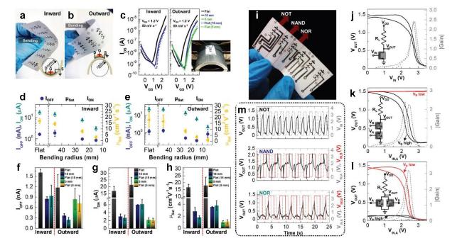
Fig. 11. a-b, Mechanical bending studies, c-e, Electrical characteristics and f-h, Transistor parameter analysis of ZnO-based TFT device. i, Optical image of ZnO-based flexible circuit. Output characteristics of j, NOT, k, NAND, and l, NOR circuit. m, Dynamic characteristics of NOT, NAND, and NOR circuits. Reprinted with permission from ref.215. © 2021 Wiley-VCH. |
Despite the positive potential of ZnO logic circuits, there are still several issues remaining to be resolved. In this situation, the main challenge is the higher defect density seen in ZnO, which has the potential to negatively affect the dependability and effectiveness of the device. The lack of a repeatable and consistent doping method, which is necessary to control the substance's conductivity, is another challenge. Additionally, as time passes, the device's functionality might degrade due to the oxidation susceptibility of ZnO. In conclusion, the unique material characteristics of ZnO logic circuits offer them a competitive alternative to traditional silicon-based technology. ZnO transistors have been proposed in a variety of device topologies, and ZnO logic circuits have been shown with the adoption of a range of manufacturing techniques. The advantages of ZnO, such as its higher electron mobility and wider bandgap, make it a favorable candidate for electrical applications that require high-speed and high-power capabilities, notwithstanding the challenges that need to be overcome.
In2O3
In2O3 semiconductor has shown promise for usage in semiconductors and other electrical components. The manufacture of In2O3 transistors has been studied using a variety of device configurations. A MIS transistor may be built using In2O3 and is the easiest kind of transistor to be built219,220. In this configuration, a thin shielding layer separates the metal gate electrode from the In2O3 channel. The effectiveness of MIS transistors is significantly influenced by the quality of the shielding coating. Shielding materials including Al2O3, HfO2, SiO2, and ZrO2 have been employed to make In2O3 MIS devices. These devices are featured with an ION/IOFF ratio of 104 and a channel velocity of 1-100 cm2 V−1 s−1 219,220. MOS transistors are similar to MIS transistors in that the gate insulator is a thin oxide layer as opposed to a metal gate conductor2221-223. The oxide layer is often produced via atomic layer deposition (ALD) or plasma-enhanced chemical vapor deposition (PECVD). MOS transistors often offer better gate control than MIS transistors because of the improved quality of the oxide layer221-223. The TFT is a typical kind of transistor configuration used in display technology. In2O3 TFTs may be created using a variety of device designs, including bottom-gate, top-gate, and dual-gate architectures3,224,225. In a bottom-gate design, the In2O3 channel, source and drain electrodes, and dual-gate designs are all put on the substrate after the gate electrode. The source and drain electrodes, as well as the In2O3 channel, are positioned on the substrate after the gate electrode in a bottom-gate design. In a top-gate design, the source/drain electrodes and gate electrode are positioned on the substrate following the In2O3 channel. Dual-gate TFTs have two gate electrodes, one at the top and another at the bottom of the channel3,224,225.
The junctionless TFTs that Yuan et al.227 disclosed were created by magnetron sputtering on transparent surfaces at room temperature, which employed In2O3 as the n-channel active layer. Due to the fact that chitosan was utilized as a gate insulator with an electric double-layer (EDL) effect, the device may function at low voltage, which reduces energy consumption. The instrument exhibited sufficient performance with a velocity of 0.21 cm2 V−1 s−1, a ION/IOFF of 106, and a subthreshold fluctuation of 66 mV/dec. The instrument maintained its performance in both dark and light situations. The system performs “OR” and “AND” logic operations with the adoption of a range of voltage values. Future applications in flexible electronics and large-area electronics are made possible by the In2O3 TFT's exceptional device performance and low production temperature. Shao et al.226 created transparent glass substrates utilizing a large area (64 × 64 array), high-resolution, and high-performance self-confined inkjet printing process.
The bilayer (IGZO/In2O3) transistors with independent bottom gates were constructed with this method. IGZO/In2O3 heterojunction channels were made using self-confined technology after IGZO dots were initially coated over UV/ozone-treated AlOx dielectric layers with diameters ranging from 55 to 70 nm and a thickness of 10 nm (Fig. 12). The resultant printed IGZO/In2O3 heterojunction TFTs have increased the mobility of 18.80 and 28.44 cm2 V−1 s−1, respectively. Furthermore, it has been shown that an IGZO/In2O3 TFT and an IGZO TFT composed of a printed NMOS converter function very well with voltage increasing up to 112. The development of a new breed of high-performance printed logic gates, circuits, and display controlling circuits may be considered as the general goal of this technology. Zhu et al.229 employed a simple, environmentally friendly aqueous solution approach to deposit a 7-nm-thin In2O3 semiconductor layer at low temperature. Then, a 20 nm or thinner ultrathin aluminum oxide insulating layer was made to manufacture high-performance devices. In addition, the advantages of ALD technology were used. Excellent electrical performance has been shown by the device, including passable mobility, a high current-to-voltage ratio, and a noticeable threshold voltage. The potential of In2O3 and AlOx TFTs was proved by the unipolar inverter. Importantly, 2.5 V was used as the working voltage to achieve all these device features.
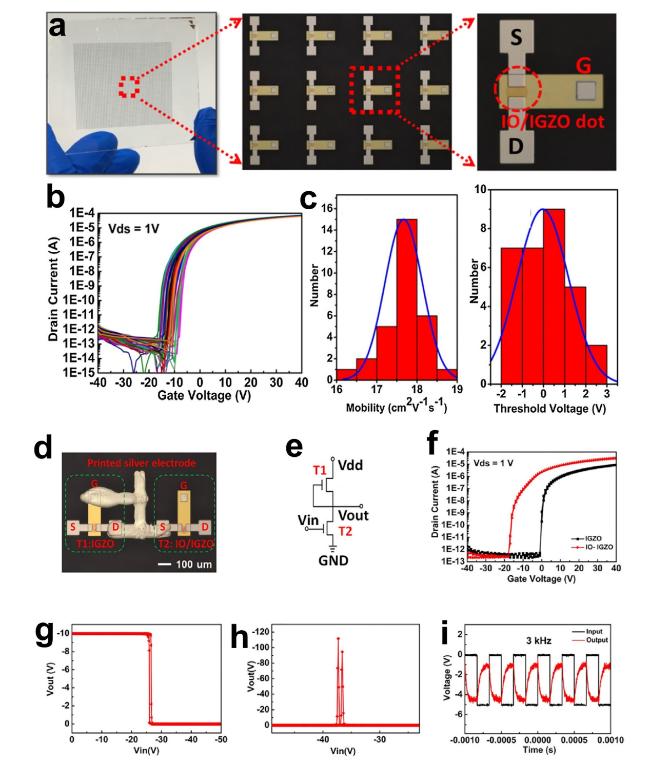
Fig. 12. a, Optical micrograph, b, electrical characteristics, and c, transistor parameters of IGZO TFT devices. d, Optical micrograph and e-i, electrical characteristics of IGZO-based NMOS inverter circuit. Reprinted with permission from ref.226. © 2021 Elsevier B.V. |
According to Xia et al.230, electrospinning was employed to create In2O3 nanofibers of exceptional purity. X-ray diffraction, scanning electron microscopy, optical spectroscopy, and electrical testing were used to analyze the form, crystallinity, optical, and electrical properties of In2O3 nanofiber surfaces. Better electrical performance was shown by FETs. Additionally, by employing the high-k Al2O3 insulating layer, the working voltage was significantly reduced (from 30 to 3 V), the mobility was noticeably raised (to 27.7 cm2 V−1 s−1), and the stability during cycling was reinforced. Wang et al.228 produced In2O3 nanofibers that were electrospun with gadolinium (Gd) and employed them as channels in the FETs. By optimizing the chemical dose and the density of the nanofibers, the device's effectiveness could be precisely regulated (Fig. 13). According to the findings, the InGdO nanofiber-based FETs with Gd doping (3%) exhibited good transistor properties. By employing high-k ZrOx as an oxide dielectric, the mobility, VTH, and SS were enhanced. In2O3-based logic circuits provide a variety of advantages over silicon-based logic circuits, including improved electron mobility, a wider bandgap, and flexibility to flexible substrates. Additionally, In2O3 is endowed with the qualities of being cheap and plentiful in the earth's crust, making it a possible replacement for silicon in developing logic circuits. It can be concluded that In2O3 shows great promise as a semiconductor material that may be used to develop high-performance logic circuitry. BJTs, logic circuits, and FETs based on In2O3 have witnessed notable developments, showing devices that are both high-speed and low power while still being reliable. The use of advanced device designs and the adjustment of fabrication process parameters may result in improved device performance. The use of In2O3-based logic circuits offers a number of advantages over their silicon-based competitors, positioning them as a potential competitor for future logic applications.
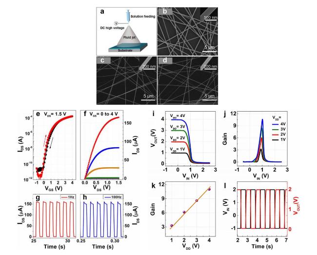
Fig. 13. a, Schematic illustration and b-d, SEM images of In2O3-based TFT device. e-f, Electrical characteristics and g-h, Dynamic response of the In2O3 TFT device. i, Output characteristics, j-k, Gain behavior and l, Dynamic response of the In2O3-based logic inverter circuit. Reprinted with permission from ref.228. © 2018 American Institute of Physics. |
IGZO
IGZO TFTs are employed in applications that require a large number of transistors to be integrated onto a single substrate, such as in the case of displays231-233. TFTs share a structural similarity with MISFETs, as both are comprised of a gate, a dielectric layer, and a channel. TFTs possess a greater channel length in comparison to MISFETs, thus facilitating a higher density of transistors on a single substrate. The present developments in IGZO transistors have predominantly focused on augmenting their performance characteristics, such as their electron mobility and their ability to withstand bias stress234, 235, 236. The investigation of advanced deposition techniques, specifically atomic layer deposition (ALD) and pulsed laser deposition (PLD), has been undertaken to produce high-quality IGZO films234,235,236. Further research efforts have been focused on improving the interface between the IGZO channel and the gate dielectric layer, to reduce leakage current and improve stability.
Kim et al.237 investigated the reliability of static and dynamic inverters, involving the utilization of a-IGZO TFTs to simulate electrical stress. The a-IGZO TFTs technology was utilized for the creation of dynamic and static converters, with the aim of assessing the dependability of electrical stress. DC and AC impulses were applied to the input of a load scenario to evaluate the dependability of the two circuits. Based on varying levels of DCHIGH, DCLOW, and AC signal stresses, the results of the tests suggest that the dynamic inverter exhibits greater electrical stability than the static inverter. The detection of gadget deterioration can also be achieved through the implementation of mechanical tension. Consequently, it will be necessary to conduct a mechanical stress analysis of the static and dynamic inverters utilizing a-IGZO TFTs.
Yang et al.7 proposed the use of an a-IGZO thin-film transistor as a translucent logic device for RFID badges. The code produced by the RFID logic device, which consists of 16 bits, was preloaded in a read-only memory. The circuits were implemented in a pseudo-CMOS logic style utilizing translucent a-IGZO TFTs. The RFID logic device that is translucent resulted in a degradation of transparency ranging from 2.5 to 8% within the frequency range of 300 to 800 nm. The utilization of a 3.2 kHz clock frequency by the RFID logic processor for the generation of Manchester-encoded 16-bit data led to a power consumption of 170 μW. The device under consideration was comprised of a total of 222 transistors and occupied a surface area of 5.85 mm2 on the silicon substrate.
The present study showcases the potential of monolithically stacked IGZO devices for compact and highly integrated circuit applications. Guo et al.238 demonstrated that a singular TFT has the capability to execute diverse logic operations through the modulation of light and electricity. This includes the “AND” and “OR” operations, which are dependent on the device's distinct responsiveness to light. The simulation incorporated excitatory postsynaptic current and paired-pulse facilitation, which are two essential simulated synaptic behaviors. The utilization of low-voltage IGZO TFTs not only enabled the construction of versatile optical devices, but also presented a novel approach to simplifying the design of programmed logic circuits.
Luo et al.239 have successfully developed optically translucent NAND, NOR gates and inverters utilizing transistors with the gate lengths of 5, 10 and 20 μm. These transistors were formed at ambient temperature and had beta ratios ranging from 2.5 to 40. The three-stage ring oscillators were able to operate at 32.87 kHz with a stage delay of 5.07 ns when supplied with a source energy of 20 V. The frequencies of operation for the NAND and NOR gates were measured up to the maximum value of 5 kHz. The study revealed that the current ION/IOFF ratios of the individual transistors were greater than 108, while their saturation mobilities were found to be 14 cm2 V−1 s−1. The successful demonstration of logic operations was achieved within 1 to 20 V for the bias voltage.
Choi et al.240 developed complementary inverters with p-type (scSWCNT) and n-type (IGZO) TFT (Fig. 14). The p-type single-chirality semiconducting carbon nanotube (scSWCNT) random network and n-type IGZO nanofiber TFTs exhibit ION/IOFF current ratios of 106 and 105, respectively. The respective threshold voltages for the two components are 7.60 and 9.50 V. Additionally, their subthreshold swings are 380.13 and 391.01 mV/dec, while their field effect mobilities for electrons and holes are 1.96 and 5.67 cm2 V−1 s−1, respectively. Furthermore, the operational mechanism of the hybrid-type inverters utilizing n- and p-channel TFTs is remarkable due to the complementary metal-oxide-semiconductor (CMOS) technology employed. It is expected that the utilization of scSWCNT random networks and IGZO nanofibers in mixed CMOS-type inverters will lead to significant advancements in open and adaptable digital logic circuits.
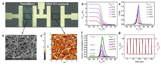
Fig. 14. a, Optical micrograph of the as-fabricated inverter circuit with insets, b, SEM and c, AFM image of the IGZO nanofibers. d, VTC, e, Gain, f, Power consumption, and g, Switching behavior of the inverter circuit. Reprinted with permission from ref.240. © 2018 American Institute of Physics. |
Transistors that employ IGZO technology offer several advantages compared to silicon-based devices. IGZO transistors demonstrate a decrease in off-state current, leading to a decrease in power consumption. Furthermore, IGZO transistors exhibit the property of transparency, rendering them appropriate to be utilized in the realm of display technology. In summary, the transformative potential of IGZO transistors in the electronics industry is attributed to their superior electron mobility, low power consumption and transparency. Indium gallium zinc oxide (IGZO) transistors have the potential to be utilized in a variety of applications due to the availability of diverse device topologies, including MISFETs, TFTs, HFETs. Recent developments in the field have focused on improving the functional characteristics of IGZO transistors, such as their durability and capacity for electron conduction. The IGZO transistors exhibit several advantages over their silicon-based equivalents, including enhanced electron mobility and reduced power consumption.
SUMMARY AND PERSPECTIVES
Overview of WBG devices-based inverter performance
Typically, integrated circuits are comprised of various logic components like inverters, NOR gates, NAND gates, and more. Thus far, inverters have been the most extensively studied circuits among WBG semiconductors. The reason behind this is that the performance of a material as an inverter can serve as an indicator of its suitability for use in integrated circuits. To gain insights into their potential in integrated circuits, a comparative analysis of inverter performance has been conducted across different WBG semiconductors (Fig. 15).
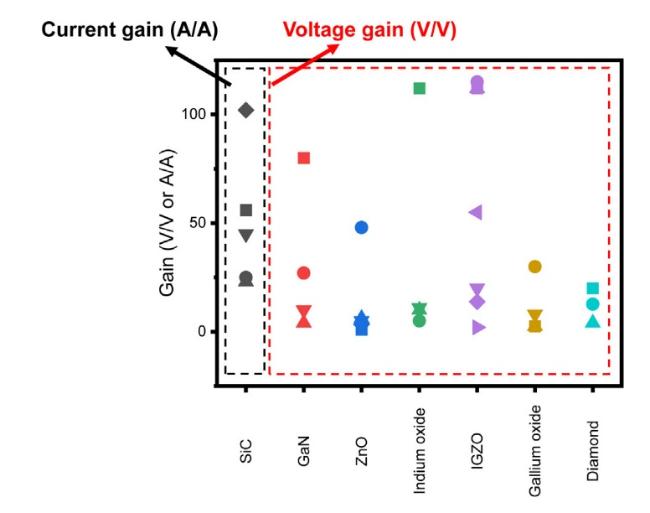
Fig. 15. Summary of current (A/A) and voltage (V/V) inverter gain of different wide bandgap semiconductors. |
Examining Fig. 15, IGZO emerges as the most robust performer among WBG semiconductors, showcasing an outstanding voltage gain of approximately 125 V/V. In general, WBG semiconductors like SiC, GaN, In2O3, and IGZO deliver commendable inverter performance, boasting gains exceeding 70 V/V. Conversely, Ga2O3 and diamond lag behind with the maximum gains of around 30 V/V and 25 V/V, respectively. This lower performance is ascribed to factors such as reduced mobility, elevated ON resistance, and high drain saturation voltage.
It is crucial to be noted that researches in Ga2O3 and diamond-based inverter technology is still in its early stages. Consequently, there exists ample scope for enhancing both device and circuit performance in the foreseeable future. Based on the latest state-of-the-art findings, we propose that IGZO and In2O3 stand out as promising wide bandgap semiconductors for constructing advanced high-performance integrated circuits.
Choice of nanomaterials over thin films in TFTs for realizing CMOS devices
The following TFT devices have nanostructures that are used to demonstrate logic circuits.
Use of CNT nanostructures in SiC CMOS
Among the many suggested molecular switching units for TFTs, single-walled carbon nanotubes (SWNTs) stand out as a prime example due to their well-documented exceptional electronic properties159. Various research groups have successfully developed logic gates based on SWNTs. However, a significant technological hurdle remains—creating air-stable ambipolar TFTs capable of both n-type and p-type behavior. This ambipolarity is crucial for building complementary logic circuits159.
Ordinarily, SWNTs tend to exhibit p-type behavior without any special treatments. This behavior arises from factors like the alignment of Fermi levels at the contact points or hole doping in the channel caused by environmental oxygen exposure. Consequently, achieving long-term stable operation under ambient conditions is a major challenge, which is mainly due to the oxidation effect in the presence of air159.
Furthermore, when constructing logic gates, it's preferable to use the Complementary Metal-Oxide-Semiconductor (CMOS) architecture. This choice is driven by the lower power consumption offered by CMOS in comparison to alternative logic families like resistor transistor logic159.
ZnO nanowire FET for 3D integrated logic circuits
Researchers have been actively exploring semiconductor nanowires (NWs) for constructing field-effect transistors (FETs) on flexible plastic substrates213. These NWs are attractive due to their unique physical properties and the ability to work with low-temperature processes. Moreover, they offer exciting possibilities like building three-dimensional integrated circuits213.
Among the various semiconductor NWs, ZnO NWs have garnered significant attention. They are well-suited for creating high-performance nanoelectronic and nanophotonic devices, thanks to their exceptional characteristics arising from their excellent crystalline structure and substantial aspect ratio213.
In this study, Kang et al.213 successfully developed logic circuits based on ZnO NWs. These circuits were constructed by vertically integrating three multilayered FETs on plastic substrates. The authors then examined the output characteristics of these CMOS logic circuits.
Electrospinning 1D In2O3 nanofibers-based transistors for logic operation
Over the past few decades, one-dimensional (1D) oxide semiconducting nanofibers have gained significant attention for their diverse applications in fields like biological sensing, energy storage, and (opto)electronics228. These nanofibers are attractive for their high mobility and unique transport properties. Integrating 1D nanofibers into electronic devices holds great promise for achieving fast operating speeds, high integrated density, and low power consumption in future nanoelectronics228.
Among the various techniques available, electrospinning stands out as a simple and cost-effective method for producing uniform and continuous 1D nanofibers. This technique offers precise control over nanofiber diameters, which can range from tens of nanometers to several microns. Additionally, it supports high-throughput production, making it ideal for mass-producing next-generation high-performance electronic devices228.
Indium oxide (In2O3) holds a prominent position as a channel material in transparent electronics due to its remarkable optical transparency in the visible spectrum and inherent high electron mobility. By harnessing the advantages of the electrospinning technique and utilizing 1D In2O3 materials, there is considerable potential to fabricate high-performance FETs that can significantly enhance logic circuit performance228.
Monolithic integration of n-channel IGZO nanofibers with p-channel CNT for demonstrating CMOS-based logic operation
Complementary inverters, consisting of n-channel and p-channel FETs, have found widespread use in digital circuits due to their advantages such as low static power consumption, large noise margins, and full voltage swing240. In-Ga-Zn-O (IGZO) has emerged as a promising candidate to replace traditional Si-based TFTs as the channel layer for n-type TFTs240. IGZO-based TFTs offer significant benefits in terms of field-effect mobility, stability, and optical transparency compared to their Si-based counterparts. However, one challenge is the mechanical flexibility of IGZO films240.
To address this flexibility issue, researchers have explored functional IGZO structures in the form of nanowires or nanotubes as an alternative to thin IGZO films240. Additionally, semiconducting single-walled carbon nanotubes (scSWCNTs) have been employed as the channel layer for p-type TFTs due to their excellent electrical and mechanical properties. Unlike traditional channel materials like poly-Si or metal oxide semiconductors, scSWCNTs can be produced through solution processing at room temperature. Moreover, they exhibit exceptional flexibility, high carrier mobility, and transparency in the visible spectrum.
In a recent study conducted by Choi and colleagues240, a hybrid-type complementary inverter was fabricated. This inverter utilized a scSWCNT network for p-type TFTs and IGZO nanofibers for n-type TFTs. This combination of materials aimed to harness the strengths of both scSWCNTs and IGZO for enhanced performance in digital circuits240.
Advantages of WBG transistors over commercial ones in IC applications
ZnO nanowires for 3D electronics
Electronic devices based on plastic substrates are gaining significant attention due to their numerous advantages, including flexibility, lightweight nature, and cost-effectiveness213. These attributes open exciting possibilities across a wide range of commercial electronics applications.
In the area of constructing field-effect transistors (FETs) on plastic substrates, substantial researches have been conducted with the adoption of semiconductor nanowires (NWs) as the active materials213. This interest stems not only from their unique physical and electrical properties but also from their compatibility with low-temperature processes213. The ability to sequentially assemble NWs offers intriguing design opportunities, such as the realization of three-dimensional integrated circuits.
Among the various types of semiconductor NWs, significant attention has been paid upon ZnO NWs owing to their potential applications in high-performance nanoelectronic and nanophotonic devices. Their extraordinary properties, which stem from their high crystallinity and substantial aspect ratio, make them particularly promising in this regard213.
ZnO TFT-based RFID tags
The widespread adoption of radio frequency identification (RFID) tags often necessitates cost reductions compared to traditional silicon complementary metal-oxide-semiconductor (CMOS) technology241. To address this, organic and metal-oxide TFTs have been proposed for RFID chip fabrication. They offer the advantage of using large-area substrates and low-temperature or roll-to-roll processing methods241.
In particular, there has been extensive researches into ZnO TFTs due to their inherent benefits, such as high mobility, the abundance of zinc materials, and their environmentally friendly characteristics. Recent work conducted by Xu and colleagues241eported ZnO TFTs with good stability and uniformity, making them well-suited for circuit-level applications.
ZnO nanowire for 1D electronics Nanowires, which are one-dimensional (1D) nanomaterials, hold significant promise as fundamental components in the development of future 1D nanoelectronic devices214. These nanowires have been applied in sensors, electronics, and optoelectronics due to their exceptional electrical properties stemming from their single crystalline structure214.
Especially intriguing are ultra-long nanowires, reaching lengths of tens of microns to millimeters and even extending to the centimeter scale, which can be synthesized using various techniques. Such extended lengths open up exciting possibilities for advanced 1D electronic and optoelectronic applications214.
Among these nanowires, ZnO nanowires are noteworthy. They typically exhibit the behavior of a WBG semiconductor with n-type characteristics, which is attributed to intrinsic oxygen-vacancy defects. ZnO is endowed with the advantage of forming ohmic contacts with a variety of metals without succumbing to oxidation issues in ambient air. Consequently, ZnO emerges as an appealing candidate for future 1D electronics applications214.
810 In2O3 TFT for transparent electronics
In recent decades, metal-oxide TFTs have garnered significant attention in the area of backplane electronics229. They are applied in active-matrix organic light-emitting diodes (AMOLEDs) and other emerging electronic technologies like complementary metal-oxide semiconductor (CMOS) devices and logic gate components, particularly on cost-effective substrates. This popularity stems from their impressive attributes, including high mobility, the ability for low-temperature synthesis, strong stability, and excellent optical transmittance when compared to traditional amorphous silicon TFTs229.
With advancements in metal-oxide semiconductor preparation techniques, solution-based methods have emerged as a pivotal approach. This method is preferred due to its simplicity, the ability to control the molar ratio of elements, cost-effectiveness, and suitability for large-scale production. Water-induced In2O3 has gained prominence as a potential channel material for transparent electronics. This is mainly ascribed to the fact that it exhibits both high electron mobility and excellent optical transparency in the visible spectrum229.
Importantly, In2O3 can display a range of electrical properties, including metallic, semiconducting, and insulating characteristics, depending on its stoichiometry and defects. When combining the advantages of the “solution route” with In2O3 materials, it becomes evident that solution-processed In2O3 holds promise as a prime candidate for fabricating high-performance oxide TFT devices at low operating temperatures229.
In2O3 nanofiber for low-power devices
Due to their highly favorable attributes like remarkable mobility and unique transport properties, one-dimensional (1D) oxide semiconducting nanofibers have been commanding significant attention in recent decades. They have been widely applied in technologies such as biological sensors, energy storage, (opto)electronics, and so on228.
Incorporating these 1D nanofibers into electronic devices holds the potential to satisfy the increasing demands for rapid operating speeds, high integration density, and low power consumption in future nanoelectronics. These nanofibers, particularly metal-oxide-semiconductor materials, are considered ideal channel materials for FETs. They have already been successfully employed in AMOLEDs, liquid crystal displays (LCDs), and other emerging electronic systems228,230.
Compared to metal oxide films, nanofibers exhibit a substantially larger active surface area, making them particularly promising. Progress in 1D nanofiber-based FETs has been instrumental in the development of asymmetric light-excited photodetectors, known for their high selectivity, sensitivity, and rapid response228,230.
Among the notable metal oxide semiconducting materials, In2O3 stands out as a leading candidate for channel materials in transparent electronics. This distinction arises from its excellent optical transparency in the visible spectrum and inherent high electron mobility. By harnessing the advantages of the electrospinning technique in combination with 1D In2O3 materials, there is considerable potential to fabricate high-performance FETs228,230.
IGZO TFT for 3D vertical integrated circuits
Since the 1960s, there has been a remarkable trend in microelectronics known as Moore's Law, which has witnessed the number of devices on microchips double approximately every two years242. This rapid advancement has been made possible by shrinking transistors, allowing more of them to be packed onto a single silicon chip. However, as the size of transistors is continuously scaled down, we have reached a point, at sub-5-nanometer scales, where the fundamental physical properties of silicon impose limitations. These limitations result in challenging second-order effects like the short-channel effect and drain-induced barrier lowering (DIBL), which are difficult to overcome. As a result, the traditional path of simply reducing transistor size is no longer viable242.
In this context, the concept of 3D integration has emerged as a potential solution to extend Moore's Law. Rather than merely reducing the size of transistors, 3D integration involves stacking components vertically, creating a three-dimensional structure. This approach can be implemented at various levels, including packaging, wafer, and device levels, with monolithic 3D integration (M-3D) being a particularly promising avenue242.
Within M-3D integration, amorphous indium-gallium-zinc oxide (a-IGZO) transistors have garnered attention. These transistors offer several advantages, including a low process temperature, high mobility (exceeding 10 cm2/Vs), and minimal leakage current (less than 10−13 A). As such, a-IGZO transistors are considered a strong candidate for powering the next generation of M-3D integrated circuits242.
Hybrid computing-in-memory system using IGZO TFT
The rapid advancement of AI models has created a growing demand for increasingly powerful hardware. In recent years, significant strides have been made in the field of computational-in-memory (CIM) with the adoption of emerging memory technologies like resistive random-access memory (RRAM). These advancements have demonstrated significantly higher energy efficiency compared to traditional computing hardware, making them highly promising for AI applications243.
While silicon complementary metal-oxide-semiconductor (CMOS) circuits can handle these operations effectively, they occupy a significant portion of chip real estate, particularly static random-access memory (SRAM) for caching, potentially diminishing the overall area efficiency of RRAM-based CIM chips243. Moreover, the frequent data transfers between RRAM arrays and caches through a bus with limited bandwidth can introduce substantial latency and limit CIM's parallelism243.
To address this challenge, there is a strong need to implement logic and cache functions in a processing-in-memory (PNM) layer using back-end-of-line (BEOL) compatible transistors and memory technologies. This layer can be seamlessly integrated directly on top of the RRAM CIM arrays, forming a hybrid CIM architecture with memory, logic, and cache capabilities. This approach enables the efficient execution of large-scale neural networks, leveraging the ultra-high bandwidth facilitated by fine-grain and densely interconnected inter-layer vias (ILVs)243.
To implement this concept, carbon nanotubes (CNTs) and indium gallium zinc oxide (IGZO) emerge as favorable channel materials for p-type field-effect transistors (PFETs) and n-type field-effect transistors (NFETs), respectively. Their advantages mainly include low processing temperatures and superior electrical performance. Additionally, CNT-FETs and IGZO-FETs can be vertically stacked in a compact configuration known as CFET, offering a reduced footprint and enhanced performance243.
Ga2O3 TFTs-based logic circuits
Power electronic devices play a crucial role in energy systems, encompassing everything from generating and transmitting electricity to storing and utilizing it183,189. These devices find applications in various fields, including electric vehicles, high-speed railways, and communication base stations. Notably, wide-bandgap (WBG) semiconductors have emerged as game-changers in the realm of power electronics183,189. They offer the ability to operate at high temperatures and withstand high breakdown voltages while delivering exceptional power conversion efficiency—qualities that traditional silicon-based power electronics struggle to achieve183,189.
Among the WBG semiconductors, β-Ga2O3 has gained considerable attention as a next-generation material for power semiconductors. Its standout feature is an ultrawide bandgap (UWBG) energy level ranging from 4.7 to 4.9 electron volts (eV), coupled with a substantial breakdown field of approximately 8 million volts per centimeter (MV/cm). Additionally, β-Ga2O3 is promising to become a cost-effective option compared to other WBG materials like GaN and SiC. This cost-effectiveness is stemmed from the relatively straightforward fabrication of high-quality, large-area single-crystalline β-Ga2O3 substrates through various growth processes such as the Czochralski method, edge-defined film-fed growth, and floating zone methods183,189.
What sets β-Ga2O3 apart are performance metrics like the Baliga figure of merit (used for evaluating power devices) and Johnson's figure of merit (assessing high-frequency power capability). In both respects, β-Ga2O3 outperforms other WBG semiconductors like GaN and SiC, making it highly suitable for crafting high-efficiency power devices and robust logic circuits. When both a power transistor and a logic driver are constructed with the adoption of β-Ga2O3, it becomes possible to create compact, high-efficiency power modules capable of withstanding high temperatures—a significant advancement in the field of power electronics183,189.
Diamond-based devices for high-temperature logic circuits
Diamond possesses a remarkable set of properties that make it an exceptional material for a wide array of applications, especially in demanding conditions such as high temperatures, high voltages, high frequencies, and intense radiation. These properties include an extensive band gap, outstanding thermal conductivity, superior carrier mobility, high breakdown field, remarkable carrier saturation velocity, and exceptional displacement energy4,152,194,201,244,245.
This unique combination of attributes positions diamond as an ideal candidate for various electronic devices used in diverse fields. These devices encompass MOSFETs, efficient heat sinks, precise detectors, advanced nuclear batteries, and applications within the realm of electrochemistry4,152,194,201,244,245.
In certain space applications, microprocessors based on GaN have been considered due to their ability to function effectively at high temperatures4,152,194,201,244,245. However, it's worthy to be noted that diamond surpasses both Si and GaN when it comes to key characteristics like bandgap, carrier mobility, and displacement energy. Consequently, diamond emerges as the superior choice for operating in extreme conditions, particularly in scenarios involving elevated temperatures and intense radiation4,152,194,201,244,245.
Given these advantages, it's imperative for future technologies to explore the integration of diamond as a replacement for silicon in microprocessors, particularly in critical domains like deep-space exploration and nuclear power plants. Diamond-based solutions hold immense potential for enhancing the performance and reliability of electronics in these challenging environments4,152,194,201,244,245.
CONCLUSION
In summary, wide-bandgap semiconductors emerge as promising candidates for transformative applications in electronics and optoelectronics, boasting significantly larger energy bandgaps compared to conventional silicon counterparts. Notable among these semiconductors are SiC, GaN, ZnO, and diamond, each distinguished by their unique attributes like heightened mobility and enhanced thermal conductivity. These properties underpin a wide spectrum of devices, encompassing energy-efficient BJTs, MOSFETs, high-frequency HEMTs, LEDs, and lasers. These semiconductors play a pivotal role in constructing integrated circuits (ICs) that drive advancements across power electronics, computer systems, RF technologies, and various optoelectronic innovations, including imaging, optical communication, and sensing.
What is of particular significance is that, the domain of power electronics has witnessed substantial advancement through the emergence of WBG semiconductor devices, which enables rapid switching of substantial currents and voltages with minimal losses. However, the integration of these devices with silicon complementary metal oxide semiconductor (CMOS) logic circuits, which is vital for intricate control functions, presents notable challenges. The endeavor to monolithically integrate silicon CMOS with WBG devices amplifies the complexity of fabricating smart ICs, which requires innovative solutions. This review proposes a strategic approach: direct implementation of CMOS logic onto the WBG platform, addressing integration complexities. Nevertheless, achieving CMOS functionalities with the adoption of WBG materials remains an ongoing hurdle, highlighting the need for further exploration.
In essence, this article encapsulates the journey of advancing integrated circuits adopting diverse WBG materials, spanning from SiC to diamond, with the overarching goal of establishing futuristic smart power ICs. This serves as a testament to the evolving landscape of technology, where the seamless convergence of wide-bandgap semiconductors and conventional circuitry holds transformative potential across myriad applications.
MISCELLANEA
Acknowledgments This work was supported by KAUST Baseline Fund: BAS/1/1664-01-01, KAUST Near-term Grand Challenge Fund: REI/1/4999-01-01, KAUST Impact Acceleration Fund: REI/1/5124-01-01.
Declaration of competing interest The authors declare that there are no competing interests.
