
INTRODUCTION
With the rapid development of the Internet of Things and artificial intelligence technology, there is a growing demand for high-speed and low-power-consumption computing. However, due to the limitation of frequent data exchange between the separated processing and memory units − the “memory wall” problem, it is difficult to improve the computing speed and power consumption in conventional von Neumann-architecture computing systems1⇓⇓⇓-5. In contrast, neuromorphic computing, such as a deep neural network (DNN) or convolutional neural network (CNN) formed by fully connected artificial synaptic device arrays, has demonstrated success in image and speech recognition with low power consumption—offering a promising approach to overcoming the memory wall problem and achieving energy-efficient computation6⇓⇓⇓⇓⇓⇓⇓⇓⇓⇓-17.
Emerging nonvolatile memory devices, such as floating gate memristors1,18⇓⇓-21, resistive random-access memristors (RRAMs)9⇓-11,22⇓⇓⇓⇓-27, electrochemical devices28,29, ferroelectric tunnel junctions (FTJs)30⇓⇓-33, and ferroelectric field-effect transistors (FeFETs)13-15,34-43 with programmable multi-state memory characteristics are promising hardware candidates to achieve neuromorphic computation. Great attention has been paid to FeFETs due to their advantageous properties of fast operation, high conductance tunability, long retention and low operating power. Thin-film-based FeFETs typically suffer from complex interfacial issues, including interfacial layers and charge traps, caused by the lattice mismatch or chemical reaction between ferroelectric and semiconductor crystals, which results in performance degradation and an increase in power consumption44. Two-dimensional (2D) semiconductors with an atomically thin nature and dangling bond-free surfaces can be stacked with ferroelectrics via van der Waals (vdW) forces to overcome interfacial problems.
To date, various ferroelectric materials (e.g., doped HfZrO2 (HZO)13,15,34⇓⇓⇓-38, LiNbO3 (LNO)14, P(VDF-TrFE)39⇓-41, α-In2Se342, and CuInP2S643 have been integrated with 2D semiconductors to build mixed-dimensional or vdW-FeFETs for neural networks. Previously, we demonstrated a vdW-FeFET adopting single-crystalline Bi4Ti3O12 (BiT) nanoflakes as a ferroelectric layer and few-layer molybdenum disulfide (MoS2) as a semiconducting channel45. Nonvolatile memory and artificial synaptic functions have been demonstrated. Several crucial synaptic characteristics are highly desired for efficient recognition: linear and symmetric conductance potentiation/depression weight update, over 100 conductance states, a low operation voltage of ≤5 V and a dynamic range of ≥100, defined as the maximum/minimum conductance ratio of Gmax/Gmin9, 46, 47.
Up till now, no FeFET that could fulfill all the requirements simultaneously has been reported. The poor linearity of the conductance weight update, which is responsible for the low recognition accuracy of a neural network, has always been obtained46,47, heavily limiting the development of neuromorphic computing hardware. Significant efforts have been devoted to improving the linearity and symmetry of the synaptic weight update. Improved linearity was achieved by carefully designing an incremental (nonidentical) pulse scheme13. A dielectric layer was inserted in the ferroelectric layer to stabilize and create more domains, demonstrated as a practical approach to improve linearity35,36. However, the improved linearity is still lower than the desired value. In contrast, the cost of the pulse design process requires additional circuit overhead.
In this study, synaptic vdW-FeFETs consisting of the single-crystalline ferroelectric, 2D semiconducting channel, and graphene vdW contacts were demonstrated, which exhibit the desired linearity and symmetry of synaptic weight update and ultra-low power consumption. The partial polarization of the multi-domain in the ferroelectric under the control of identical voltage pulses was experimentally explored. The desired synaptic weight update with high linearity (|NLp| ∼ 0.016, |NLd| ∼ 0.013) and symmetry (|NLp| − |NLd| = 0.003) has been demonstrated with our vdW-FeFET under an identical pulse scheme. Other critical synaptic device specifications, such as ≥128 conductance states, low operation power of <10 fJ/spike and operation voltage of ≤5 V, were also achieved in the desired regions. Simulations were also applied for Modified National Institute of Standards and Technology (MNIST) handwritten digit recognition and electrocardiogram (ECG) pattern recognition with our vdW-FeFET, with high accuracies of 97.6% and 92.4%, respectively. Such excellent device performance emphasizes the advantage of vdW-FeFET for achieving high-precision neuromorphic computing.
RESULTS AND DISCUSSIONS
Full vdW-FeFET
The schematic of a fabricated vdW-FeFET is shown in Fig. 1a. It consists of an 8-nm-thick few-layer MoS2 semiconducting channel and a 300-nm-thick BiT ferroelectric layer (see Fig. S1 for atomic force microscope image). Here, the BiT nanoflake was chosen over the layered CIPS for several reasons. Firstly, BiT nanoflakes exhibit a much higher Curie temperature (over 950 K) than CIPS (∼315 K), making them more suitable for high-temperature applications. Additionally, BiT nanoflakes are of excellent air stability, which is important for ensuring long-term device performance. The few-layer graphene was adopted as the vdW contacts to reduce device power consumption, owing to the merit that it could offer high-quality electrical contacts to MoS2 with a negligible Schottky barrier, i.e., a low contact resistance48. Fig. 1b presents the transfer characteristics of the vdW-FeFET measured at a drain bias of Vds = 100 mV. An anticlockwise hysteresis window with a size of 25 V was measured with an on/off of 106, indicating the formation of the FeFET. The abrupt switch-on and switch-off were read at Vg = 12 V and Vg = −13 V, corresponding to electric fields of 0.40 MV/cm and −0.43 MV/cm, where BiT was downward and upward polarized. In this study, six vdW-FeFET devices were fabricated and measured. Their characteristics, which exhibit high repeatability, are summarized in Table S1.
Voltage-pulse controlled partial polarization of multi-domain ferroelectric
Such a FeFET device can mimic a synapse when the ferroelectric possesses the multi-domain feature. The physical mechanism of the FeFET synapse is illustrated in Fig. 1c. For instance, for an up-polarized BiT, the MoS2 channel is switched off by the electrostatic doping effect. The pre-synapse stimulations were mimicked with the electrical pulses applied at the gate, whereas the postsynaptic current (PSC) was defined by the channel current. When applying a sequence of positive gate voltage pulses, the partial polarization reversal of the multi-domain structure is triggered. Subsequently, the MoS2 channel is gradually switched on by electrostatic n-type doping of the reversed domains. Eventually, more domains are down-polarized with the increased numbers of gate pulses, and the FeFET is tuned into the higher conductance state—similar to the excitatory behavior of a neuron synapse. The inhibitory behavior can be evoked by applying the negative pulses.
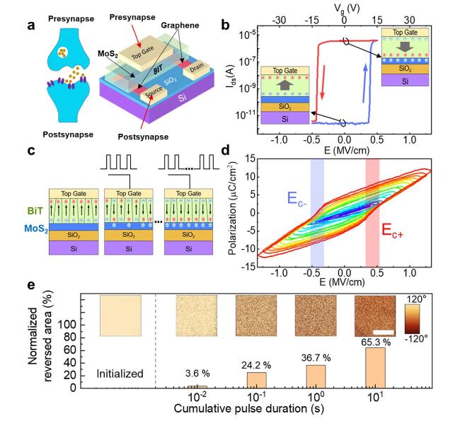
Fig. 1. vdW-FeFET artificial synaptic device and the partial polarization reversal of multi-domain BiT. a, Schematic illustration of the vdW-FeFET synaptic device. b, Ids-Vg transfer characteristic measured in vdW-FeFET. The source-drain bias Vds = 100 mV. Inset: Schematics of the full polarizations of FE in the on-state and off-state. c, Schematic of multi-domain and partial FE-polarization switching in vdW-FeFET. d, The P-V curves were measured using an metal-ferroelectric-metal (MFM) device. The blue and red shadows indicate the distributions of the coercive fields in the up-and-down polarization. e, The partial polarization reversal probed by the PFM technique and the corresponding reversed area at specific cumulative pulse durations extracted from the PFM images. The scale bar is 1 µm. |
The multi-domain feature of BiT was described. Multi-domain ferroelectrics possess dispersed coercive fields when changing the poling field range as an aggregate response of the distribution of multiple ferroelectric domains with discrete and deterministic coercive fields and inhomogeneous ferroelectric domain nucleation13,36. This response was verified by measuring the polarization-electric field characteristic of BiT with a metal-ferroelectric-metal (MFM) capacitor (Fig. 1d). The MFM capacitor was fabricated using the few-layer graphene as the bottom electrode and indium/gold stack deposited on the top of BiT as the top electrode. The quartz substrate was adopted to suppress parasitic capacitance. A wide dispersion of coercive field from ±0.3 to ±0.6 MV/cm (red and blue rectangles) are observed, and the remnant polarization remains unsaturated up to ±8 µC/cm2, indicating the existence of multiple domains. The partial reversal of ferroelectric polarization can be visualized by step-by-step switching measurement using a piezoresponse force microscope (PFM, NanoMan VS) on a 300-nm-thick electrode-free BiT surface.
Firstly, a negative voltage bias of −10 V, corresponding to an electric field of −0.33 MV/cm, was applied to BiT to initialize all domains to up-polarization. Subsequently, a sequence of positive voltage pulses of +5 V was applied, which is lower than the coercive voltage and triggers the partial reversal of the domains. By measuring the PFM images after specific numbers of pulses, the gradual switching of ferroelectric domains is observed, as presented in Fig. 1e. When applying positive pules, the up-polarization initialized domain separates and splits into many small domains with opposite polarizations caused by the inhomogeneous nucleation of new up-polarized domains30, 49, 50.
A single 10 ms pulse reverses 3.6% of domains in the downward direction. The reversed area increases with the cumulative pulse durations, while the ratio of the reversed area reaches ∼65% with cumulative 10-s pulses. A linear relationship exists between the reversed area and the logarithm of cumulative pulse duration, which is consistent with previous studies30,51. The PFM results provide definitive experimental evidence for electrically controlled partial polarization reversal in BiT, which is critical to achieving multi-state memory and synaptic plasticity of vdW-FeFETs.
Programming of multi-state FeFET memory
Multi-state memory behavior can be achieved by electrically controlling the polarization status of ferroelectric domains in the vdW-FeFET. Based on the previous measurements, the program/reset pulse scheme was designed to achieve multi-state memory, as illustrated in the top panel of Fig. 2a. Firstly, a −20 V gate bias with a duration of 10 s was applied to initialize the vdW-FeFET to the off state, denoted as S1. Drain current Ids was measured under dual gate voltage sweeping from +10 V to −10 V to characterize the conductance state. A program gate voltage pulse of +10 V (slightly smaller than the full-polarization switching voltage) with a duration of 5 s was applied to tune a discrete level of partial down-polarization, which changes the n-doping level and the conductance of the MoS2 channel. Subsequently, cumulative program pulses could define the discrete conductance states from S2 to S5 with increased conductance, as plotted in Fig. 2b. Similarly, a sequence of reset gate voltage pulse of −10 V with a duration of 5 s could gradually reverse the ferroelectric domains in up polarization, reducing the n-doping concentration in the MoS2 channel and resetting the conductance states from S5 back to S1.
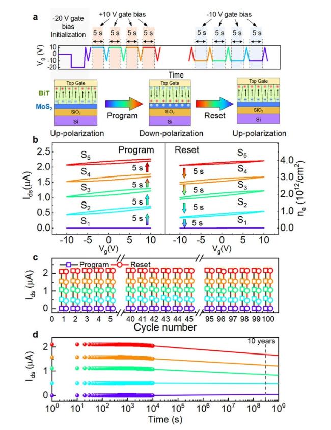
Fig. 2. Gate bias programmed multi-states characteristics. a, Schematic illustration of the program/reset sequence in the measurement (top) and gate bias duration induced partial polarization of ferroelectric domains in vdW-FeFET (bottom). b, Ids-Vg characteristics measured after 5 to 20 s of the program (left) and the reset (right) sequence with a step of 5 s in bias duration. c, Ids read at Vg = 0 V, Vds = 100 mV in the 100 program/reset cycles. d, The retention characteristic of S1 to S5. |
The gate bias duration modulated carrier density in vdW-FeFET was evaluated to examine multi-state memory characteristics. In the program sequence, the carrier density was increased from S1 at a rate of 1 × 1012 cm−2 per operation, reaching 4 × 1012 cm−2 at S5. The observed multi-state memory behavior is quantitatively consistent with the PFM-probed partial polarization. The conductance and carrier density changes as a function of gate bias duration are plotted in Fig. S2. The linear change in carrier density after each gate operation is a critical feature of multi-state memory.
The reliability of the device as a nonvolatile multi-state memory was examined by performing endurance and retention tests. The results are depicted in Fig. 2c and Fig. 2d. The endurance test is performed by applying over 100 cycles of the periodic program and reset pulses as defined in Fig. 2a. Stable switching between the five conductance states is observed with negligible fluctuation over multiple operations, indicating high endurance. Moreover, each discrete conductance state lasts over 10000 s in the retention measurements (Fig. 2d), providing strong evidence suggesting the potential application of the vdW-FeFET as nonvolatile memory.
High-performance artificial synapse
The highly tunable multi-state memory behavior in the vdW-FeFET can be used to mimic synaptic plasticity. The gate and drain contacts were defined as the pre-synapse and the post-synapse. A low source-drain bias Vds of 1 mV was applied to sustain low power consumption. An identical pulse scheme with an amplitude of ±5 V, a pulse width of 50 ms and an interval of 50 ms was used for the pre-synaptic spikes. The relaxation of PSC was also monitored by measuring PSC after “n” pulses of +5 V and “m” pulses of −5 V (n, m = 1, 5, 10, 15, …, 30) for 1.4 s; the results are presented in Fig. 3a. The device is set to the off-state first. The updated PSC can retain without returning to its initial state, exhibiting short-term plasticity behavior. In the previous experiments, an extended relaxation time of over 100 s, caused by the nonvolatile nature of ferroelectrics, was demonstrated45, which is beneficial to the implementation of inference in the neural network.
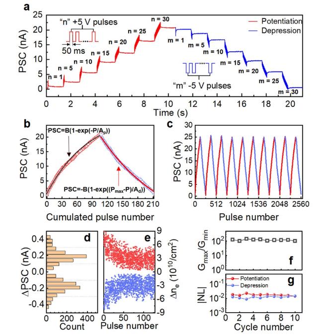
Fig. 3. Synaptic performance of vdW-FeFET. a, The PSC weight during potentiation (red) and depression processes. “n” denotes the number of pulses of individual potentiation and depression pulse train. b, Non-linearity factor fitting with summarized PSC weight update in a. c, Cycle-to-cycle potentiation and depression with 128 conductance states. d, Count distribution of PSC and ne change (ΔPSC and Δne). e, ΔPSC and Δne variation in the cycle-to-cycle weight update measurement. f, The dynamic range Gmax/Gmin and g, the non-linearity |NL| variation extracted from c. The Vds is set to 1 mV during these measurements. |
With the cumulative positive pre-synaptic spikes, the PSC was eventually increased to 21 nA after 106 pre-synaptic spikes, indicating the transition from a short-term to long-term potentiation. Similarly, the cumulative negative pre-synaptic spikes contributed to a short-term to long-term depression transition. Fig. 3b summarizes the PSC weight update of the potentiation and depression processes extracted from the data plotted in Fig. 3a. By fitting the PSC weight update to an exponent equation (Supplementary Note S1), the non-linearity factor |NLp| ∼ 0.016 for potentiation and |NLd| ∼ 0.013 for depression was extracted. To our knowledge, compared with other FeFETs and two-terminal ferroelectric nonvolatile memory synaptic devices, these non-linearity values are among the lowest values.
Besides the non-linearity factor, the cycle-to-cycle, device-to-device variation and dynamic range Gmax/Gmin are essential for high recognition accuracy46,47. Fig. 3c illustrates 10 operation cycles of 128-state potentiation and depression processes to meet the 7-bit computing requirement. The distribution of ΔPSC measured in various cycles is plotted in Fig. 3d and Fig. 3e. The cycle-to-cycle variation is defined as the ratio of PSC change (ΔPSC) and PSCmax − PSCmin. Subsequently, a low mean cycle-to-cycle variation of 0.8% is obtained, while the maximum variation value is about 2%. Low power consumption is estimated to be ∼10 fJ/spike using the equation Vds × ΔPSC × t, where Vds = 1 mV is the bias voltage, ΔPSC = 0.2 nA is the mean PSC weight update per spike, and t = 50 ms is the spike duration20,52,53. The fastest operation is limited to 50 ms by our instrument. In principle, FeFETs could enable faster operation up to several tens of nanoseconds54. Consequently, much-improved device performance and lower power consumption are expected with the vdW-FeFET.
The variation in the dynamic range Gmax/Gmin and non-linearity in the cycle-to-cycle measurement is summarized in Fig. 3f and Fig. 3g. The Gmax/Gmin > 120 and |NLp,d| ranging from 0.009 to 0.022 are confirmed. The variation in dynamic range and non-linearity is evaluated by analyzing Gmax/Gmin, |NLd| and |NLp|, calculating their standard deviations as 13.56, 0.0018 and 0.0022, and their means as 120.8, 0.0123 and 0.0175. The standard deviations are one order of magnitude smaller than the means, implying the uniform and repeatable characteristics of LTP/LTD. Furthermore, a low device-to-device variation of 0.7% is obtained by calculating the standard deviation of |NL| extracted from the all six fabricated vdW-FeFETs (see Table S1).
Pattern recognition using vdW-FeFET-based artificial neural network
In order to confirm the advantages of vdW-FeFET in high-precision neuromorphic computing applications, a supervised learning simulation of an artificial neural network based on a back-propagation algorithm was conducted using the open-source simulator NeuroSim MLP 3.0 in the LINUX environment46,47. The MNIST handwritten digit dataset was used for the simulation. Fig. 4a illustrates the schematic of a vdW-FeFET pseudo-crossbar array used to build the two-layer neural network in the simulation. The neural network consists of 784 input neurons, 300 hidden neurons and 10 output neurons. The 784 input neurons and 10 output neurons correspond to the 28 × 28 pixels MNIST image and the digits from “0” to “9”. The vdW-FeFET were used as individual cell devices in the pseudo-crossbar array, and the measured PSC weight update data were adopted as the synaptic weight update for the implementation of MNIST recognition.
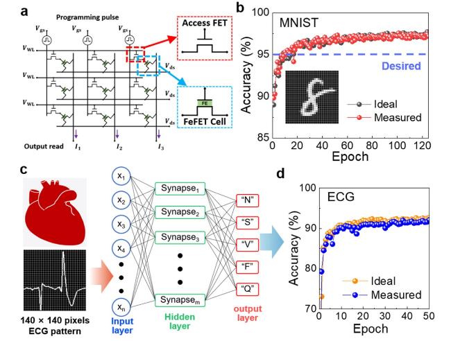
Fig. 4. MNIST digits and ECG pattern recognition. a, The structure of the vdW-FeFET-based pseudo-crossbar array used to build the artificial neural network. b, The MNIST recognition accuracy as a function of training epochs. c, The schematic of the neural network used for ECG pattern recognition simulation. d, The accuracy of ECG pattern recognition simulation as a function of training epochs. |
Based on the non-linearity factor, state number, Gmax/Gmin, cycle-to-cycle and device-to-device variation parameters (Fig. 3), The recognition accuracy of 97.07% was achieved after 50 training epochs and the maximum accuracy of 97.59% was realized after 100 epochs. Furthermore, the accuracy was maintained at the mean value of 97.05% after 50 epochs, which is close to the ideal device hardware at 97.11% (Fig. 4b). Consequently, state-of-the-art synaptic device performance was achieved.
In addition to the simple MNIST digit recognition, the artificial neural network can also be applied to classify the ECG patterns55. The ECG patterns can be categorized into five classes, which are denoted as “N”, “S”, “V”, “F”, and “Q”. Each class of ECG patterns corresponds to normal or different abnormal heartbeats. Hence, accurate ECG recognition leads to promising applications in diagnosing cardiovascular diseases. Its feasibility was verified by an ECG recognition simulation. Single-period ECG data from the MIT-BIH Arrhythmia Dataset were selected and converted into images of 140 × 140 pixels for the ECG recognition simulation (Fig. 4c). Accordingly, the input layer of the neural network is customized to 140 × 140 neurons, which are connected to 300 hidden neurons. The number of output neurons is reduced to five corresponding to five typical heartbeat classes denoted as “N”, “S”, “V”, “F”, and “Q”.
The recognition results are presented in Fig. 4d. A high recognition accuracy of over 90% is achieved after 8 back-propagation epochs using the measured data, and it reaches >92% after 40 epochs, which is ∼2% lower than the result achieved using the ideal devices. Since most of the ECG patterns are similar, the accuracy of ECG recognition is lower than that of the MINST digits. Nevertheless, compared with the previously reported value with an organic FeFET-based single-layer neural network, an increase in accuracy by ∼20% was still achieved by the vdW-FeFET neural network in the current work56.
Metric benchmarking of recent advances
Fig. 5 presents the benchmarking of the device performance metrics of recently developed artificial synaptic devices for comparison, including three-terminal devices such as 2D FETs18, thin film-based, and 2D materials-based FeFETs13,35-43, as well as two-terminal devices such as filamentary RRAM22-27, FTJs30, 31 and organic synaptic devices1,26,28,29. An overall view of the development of high-performance synaptic devices was presented by the empirical roadmap in Fig. 5a. The trend of the roadmap shows the importance of optimizing Gmax/Gmin and non-linearity for achieving higher accuracy, which is consistent with the simulation prediction13,44,45. The ideal accuracy limitation changes with different simulators, e.g., a higher ideal accuracy limit of ∼99% can be realized using the simulator CrossSim32, 40.
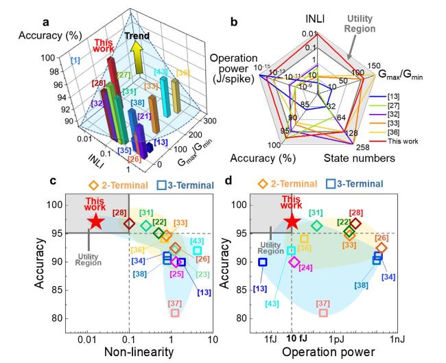
Fig. 5. Metrics benchmarking of the recently developed synaptic devices. a, An empirical roadmap of the trend to achieve higher accuracy. b, Radar plot of our vdW-FeFET device performance results compared with state-of-the-art synaptic devices. c-d,present the overall metrics benchmarking of the latest synaptic devices in different references in terms of accuracy, non-linearity, and operation power. The empty diamonds denote two-terminal devices, and squares denote three-terminal devices, respectively. |
The radar plot in Fig. 5b indicates that the vdW-FeFET could fulfill all required synaptic device performance metrics, such as dynamic range, operation power, state number, non-linearity and recognition accuracy. Moreover, the benchmarking of device performance metrics depicted in Fig. 5c and Fig. 5d confirms that the vdW-FeFET is of lower power consumption than other two-terminal synaptic devices, and higher accuracy than other three-terminal devices. These devices with Gmax/Gmin < 10 are not included since the poor dynamic range conflicts with the development trend toward high accuracy13,44,45. The synaptic device comparison is summarized in Table S2.
CONCLUSIONS
In this work, an all-round synaptic device was experimentally demonstrated based on a vdW-FeFET. The working principle of the vdW-FeFET synapse is based on the partial switching of multiple ferroelectric domains under electric pulses, explored using both electrical and PFM measurements. The vdW-FET exhibits a stable multi-state memory behavior, a highly desired linear PSC weight update, an extensive dynamic range and a high number of conductance states. Most importantly, the linear PSC weight update was achieved under an identical pulse scheme to facilitate practical and straightforward applications. The benchmarking reveals low linearity, a large state number and a high dynamic region, leading to high recognition accuracy. Furthermore, the vdW-FeFET meets the requirement of low-power operation with 10 fJ/spike. The image recognition simulation suggests that a high accuracy of >97% was realized based on the measured device characteristics after training on the MNIST database. More importantly, recent advancements in the development of transferable single crystalline ferroelectric oxides and van der Waals transfer techniques enables the feasibility of the large-scale fabrication of vdW-FeFETs56, 57. These superior device performance metrics highlight the advantages of vdW-FeFET for developing an energy-efficient high-precision neural network.
METHODS
Materials synthesis
Single-crystalline BiT nanoflakes were synthesized through the molten-salt method. Stoichiometric amounts of bismuth (III) oxide (Bi2O3) and titanium dioxide (TiO2) powders with the purity of 99.9% were mixed thoroughly by ball milling in ethanol for 12 h. Equal amounts of sodium chloride (NaCl) and potassium chloride (KCl) (1:1 mol) were added as salts. The dried mixtures were heated to 900 ℃ and maintained for 2 h. The low temperature of 900 °C reduced the density of oxygen vacancies in BiT. The salts in the products were carefully removed by washing the samples several times with hot deionized water.
Device fabrication
Device fabrication starts with the preparation of the graphene contact. Graphene flakes were mechanically exfoliated from single-crystal highly oriented pyrolytic graphite and transferred onto a heavily doped silicon substrate capped with a 285-nm-thick SiO2 layer. Two adjacent few-layer graphene flakes were selected as contacts. A several-layer MoS2 flake was exfoliated on a polydimethylsiloxane (PDMS) stamp and then transferred on the top of graphene contacts. The synthesized BiT was then dispersed on a PDMS stamp and transferred to the top of the MoS2 as the ferroelectric layer. Finally, a 10 nm/50 nm indium/gold stack was metalized on the graphene contacts and gate using a thermal evaporator to form the electrical contact pads. The MFM capacitor was fabricated adopting the few-layer graphene as the bottom electrode and indium/gold stack deposited on the top of BiT as the top electrode. The quartz substrate was used to suppress parasitic capacitance. The PFM measurements were conducted using a NanoMan VS piezoresponse force microscope. The electrical characterization of the vdW-FeFET was conducted in a vacuum environment at the pressure below 0.1 Pa.
Artificial neural network simulations
Simulation of the artificial neural network was conducted using the open-source simulator NeuroSim MLP 3.0 in the LINUX environment. The MNIST handwritten dataset and ECG heartbeat dataset from the MIT-BIH Arrhythmia Dataset were used in the simulation. The pattern recognition simulations were implemented in a pseudo-crossbar structure, as illustrated in Fig. 4. The performance of synaptic cells was simulated based on the experimentally measured LTP/LTD data, cycle-to-cycle variation and device-to-device variation factors. The network size was set to 784 × 300 × 10 for the 28 × 28 (pixels) MNIST images and at 19,600 × 300 × 5 for the 140 × 140 (pixels) ECG images. At each epoch, the neural network was trained on patterns from a 60,000-image training dataset, and the recognition accuracy was tested in a separate 10,000-image testing dataset.
MISCELLANEA
Supplementary materials Supplementary material associated with this arti- cle can be found, in the online version, at doi:10.1016/j.chip.2023.100044.
Declaration of Competing Interest The authors declare that they have no known competing financial interests or personal relationships that could have appeared to influence the work reported in this paper.
