图/表 详细信息
Implementing hardware primitives based on memristive spatiotemporal variability into cryptography applications
Chip,
2023, 2(1):
100040-12.
DOI: 10.1016/j.chip.2023.100040
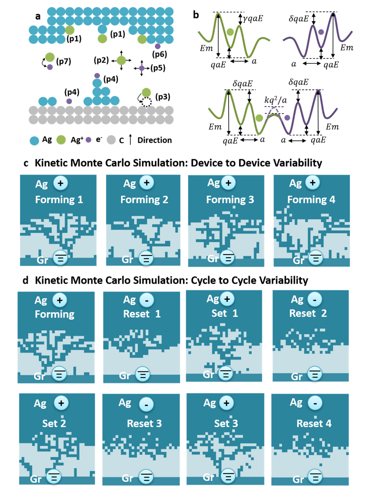
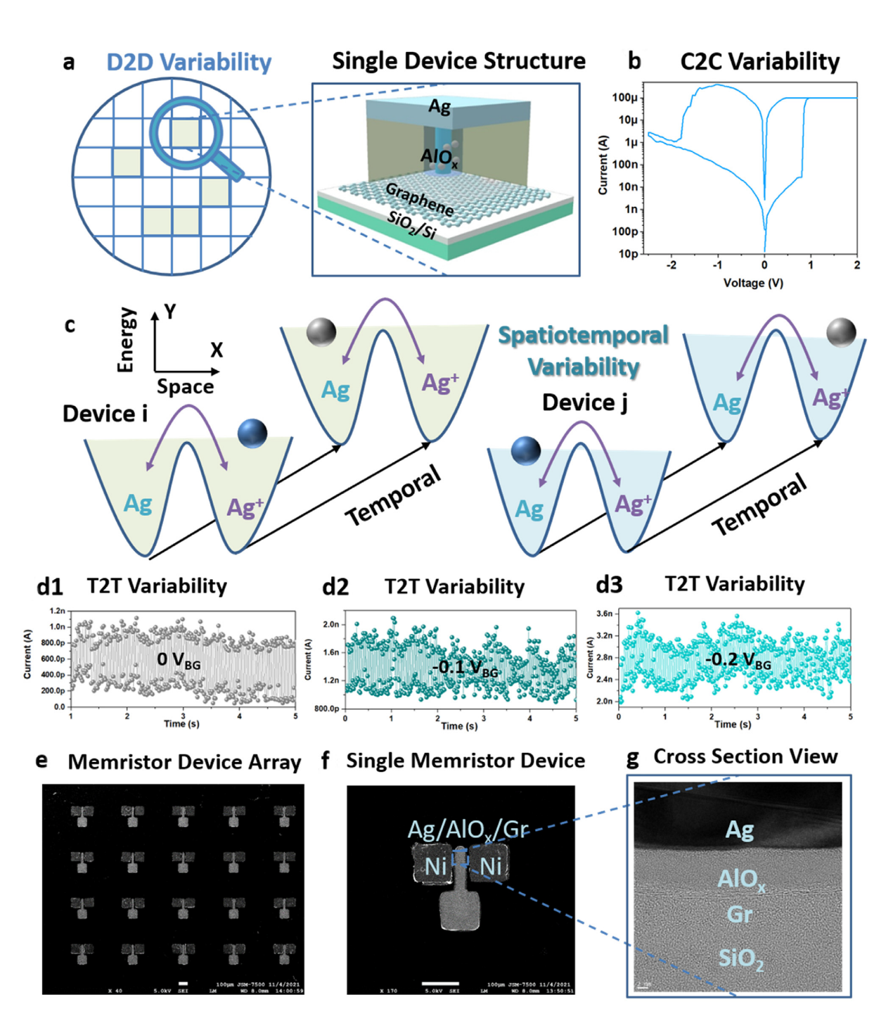
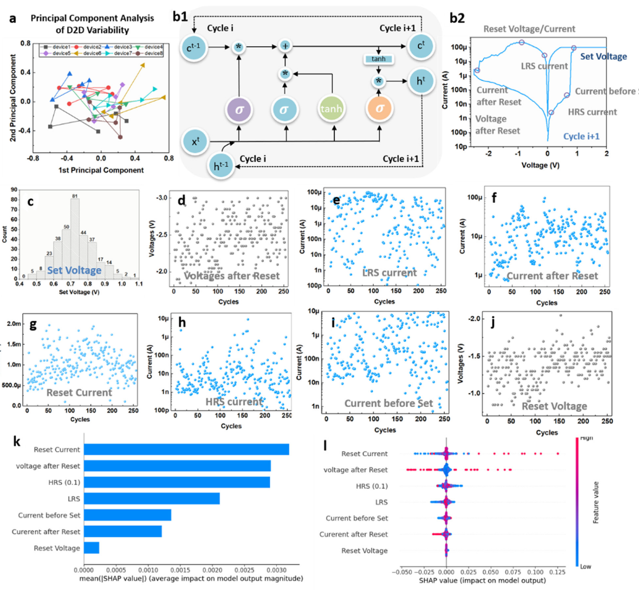
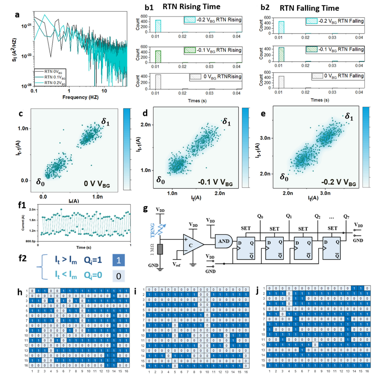
Fig. 2. Kinetic Monte Carlo simulation of graphene CBRAM for visualising DDV and CCV. a, Schematics of the device structure and the holistic filament revolution; including p1: anode oxidation, p2: cation hopping, p3: cation reduction and deposition on cathode, p4: electron emission, p5: electron hopping, p6: electron adsorption, p7 cation and electron reduction. b, Electric field alter the migration barrier of cation and electron; and the reduction of the cation and electron. c, Filament morphology of four different devices after forming process. d, Filament morphology of 4 cycles of Set and Reset, including the first forming process.
本文的其它图/表