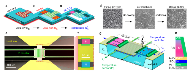
The fabrication process of the on-chip TE TCers is shown in Fig. S1. Beginning with a 1 × 1 cm
2 silicon/silicon nitride (Si/Si
3N
4) substrate, including ~ 300-μm-thick Si and ~ 100-nm-thick double-sided Si
3N
4 layers, the Si
3N
4 layer was partially etched by reactive ion etching (RIE) using CF
4 gas under the protection of the patterned photoresist. The freestanding Si
3N
4 window was obtained after removing the Si layer in the 40% KOH at 353 K for ~ 300 min. Second, temperature sensor electrodes (Pt/Ti, 38/6 nm, marked by green in
Fig. 1e-h) were deposited on the Si
3N
4 window using standard lithography, magnetron sputtering, and lift-off process, followed by a 50-nm-thick Atomic Layer Deposition (ALD) of SiO
2 at 473 K as an insulation layer. Next, the photoresist was lithographically patterned on the SiO
2 layer, to open the electrodes for performance measurement by RIE with CF
4 gas. Third, working electrodes (Au/Cr, 180/20 nm, marked by yellow in
Fig. 1e-h) can be obtained by sputtering and patterned etching. It is worth noting that the key role of the above SiO
2 layer is to insulate the Pt sensor and Au working electrodes in TCer (illustrated in the multilayer structure in
Fig. 1g). Fourth, the unnecessary parts of the Si
3N
4 window together with SiO
2 are thoroughly etched by RIE with CF
4 gas to ensure good thermal insulation conditions for the μ-TCer. Finally, the individually prepared n- and p-type freestanding Bi
2Te
3-based TE thin films (Sect. 2.1) were integrated onto the above-prepared chips by the focused dual-beam technique (FEI, Helios 600i). The integrated on-chip μ-TCer is shown in the SEM image (
Fig. 1e, f) and the corresponding 3D schematic (
Fig. 1g, h), details in Tables S1 and S2. The PPMS system can provide a high vacuum (~ 0.01 mTorr) and accurate ambient temperature setting (280−380 K) for the performance test of our μ-TCers (similar to the operating temperature range of microelectronics). A Pt temperature sensor was used to assess the temperature controllability of our TCers (Fig. S3). Heat-compensation method (dual currents) was used for the cooling power and efficiency test, one is the working current (
Iw), and another one is the heating current (
Ih) to simulate the Joule effect of the micro components and simultaneously monitor the real-time temperature, details in Sect. S1.2.


