HIGHLIGHTS
1 Introduction
2 0D TMCs
2.1 Principles of Ion Exchange Reactions
Table 1 Comparison of bond dissociation energies (BDEs) of some metal chalcogenides |
| Compound | BDEs (kJ mol−1) | Compound | BDEs (kJ mol−1) |
|---|---|---|---|
| Ag2S | 216.7 ± 14.6 | CdSe | 127.6 ± 25.1 |
| Ag2Se | 210.0 ± 14.6 | CdTe | 100.0 ± 15.1 |
| Ag2Te | 195.8 ± 14.6 | ZnO | 280.1 |
| Cu2O | 259.0 ± 30.0 | ZnS | 224.8 ± 12.6 |
| Cu2S | 274.5 ± 14.6 | ZnSe | 170.7 ± 25.9 |
| Cu2Se | 255.2 ± 14.6 | ZnTe | 117.6 ± 18.0 |
| Cu2Te | 230.5 ± 14.6 | PbS | 398.0 |
| CdO | 236.0 ± 84.0 | PbSe | 302.9 ± 4.2 |
| CdS | 280.5 ± 20.9 | PbTe | 249.8 ± 10.5 |
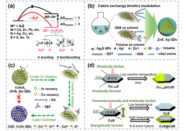
Fig. 1 Schematics of ion exchange reaction principles a Thermodynamic scheme of the cation exchange (CE) reactions initiated by the phosphine ligands. Reproduced with permission [65]. Copyright 2015, John Wiley and Sons. b Schematic of the thiol ligands and solvents combination coordinated CE reactions. Reproduced with permission [66]. Copyright 2019, John Wiley and Sons. c Schematic of CE reaction triggered by surface vacancy engineering. Reproduced with permission [67]. Copyright 2020, Elsevier. d Scheme of partial CE reactions in djurleite Cu1.94S nanodisks and covellite CuS nanodisks. Reproduced with permission [68]. Copyright 2022, RSC Pub |
2.2 Complete Exchange
2.2.1 Syntheses of 0D TMCs via CE Reactions
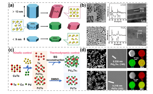
Fig. 2 Synthesis and characterizations of 0D TMC materials obtained by CE reactions. a Schematics of height-dependent phase transformation of Cu1.8S nanocrystals during the CE process and b corresponding transmission electron microscopy (TEM) images, X-ray diffraction (XRD) patterns, high-resolution transmission electron microscopy (HRTEM) images. Reproduced with permission [38]. Copyright 2021, The American Association for the Advancement of Science. c Schematic showing the kinetic control and thermodynamic control for the CE process of PdTe and Pd20Te7 nanospheres synthesis. EG represents ethylene glycol and DMSO represents dimethyl sulfoxide. d TEM, HRTEM images of PdTe2 and Pd20Te7 nanospheres and corresponding energy-dispersive X-ray spectroscopy (EDS) elemental mapping images. Reproduced with permission [60]. Copyright 2022, Springer Nature |
Table 2 Representative examples of reported core@shell heterostructures with different lattice mismatches |
| Core | Shell | Lattice mismatches (%) | Overall morphology | Refs. |
|---|---|---|---|---|
| PbTe | CdTe | < 1 | Sphere | [29] |
| PbSe | CdSe | ~ 1 | Sphere/rod/cube | [82, 83] |
| PbS | CdS | ~ 2 | Rod/sphere | [84, 85] |
| CuInS2 | ZnS | 2-3 | Sphere | [86] |
| CdSe | CdS | 3.8-3.9 | Rod/sphere/tetrapod | [87, 88] |
| CdTe | ZnTe | 6.5 | Sphere | [89] |
| CdTe | CdSe | 6.7-7.1 | Sphere/prolate-shape | [90, 91] |
| CdTe | ZnS | 19.8 | Sphere | [89] |
| Ag | CdS | 35.3 | Triangle | [92] |
| Au | CdS | 42.7 | Sphere | [69] |
| Pt | CdS | 48.3 | Sphere/cube | [65, 69] |
| Au | CdSe | 49.1 | Sphere/dumbbell | [69, 93] |
| Au | CdTe | 58.9 | Sphere/rod | [69, 94] |
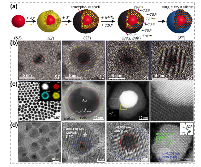
Fig. 3 Synthesis and characterizations of 0D metal-semiconductor heterostructures obtained by the reverse CE reaction-facilitated non-epitaxial growth strategy. a, b Schematic showing different growth stages of Au@CdS heterostructures and the corresponding HRTEM images. Reproduced with permission [69]. Copyright 2010, The American Association for the Advancement of Science. c TEM images of Au@ CdS heterostructures and high-angle annular dark-field scanning TEM (HAADF-STEM) images with corresponding elemental mapping images. Reproduced with permission [48]. Copyright 2018, Elsevier. d TEM and HAADF-STEM images of Au@CdS/CsPbBr3 heterostructures. Reproduced with permission [71]. Copyright 2022, John Wiley and Sons |
2.2.2 Syntheses of 0D TMCs via AE Reactions
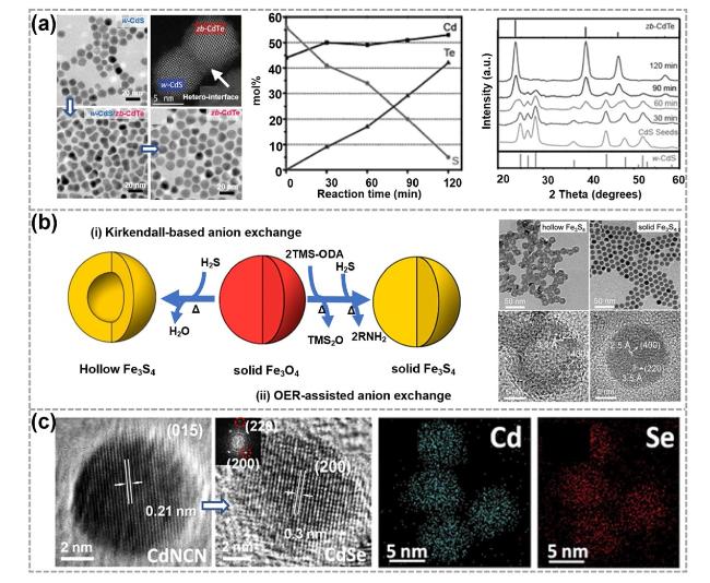
Fig. 4 Synthesis and characterizations of 0D TMC materials obtained by the anion exchange (AE) reactions. a Synthesis illustrations of w-CdS/zb-CdTe heterodimers and corresponding TEM and HAADF-STEM images. Reproduced with permission [96]. Copyright 2011, American Chemical Society. b Illustrations showing the synthesis of hollow Fe3S4 and solid Fe3S4 nanocrystals and corresponding TEM and HRTEM images. OER represents an oxygen extracting reagent, TMS-ODA represents (Z)-N-trimethylsilyloctadec-9-en-1-amine and TMS2O represents bis-(trimethylsilyl) oxide. Reproduced with permission [97]. Copyright 2020, American Chemical Society. c Illustrations showing the synthesis of MX nanoparticles (M = Cd, Mn; X = S, Se) and corresponding HRTEM image as well as EDS elemental mapping images. Reproduced with permission [98]. Copyright 2019, American Chemical Society |
2.3 Partial Exchange
2.3.1 Synthesis of 0D Doped TMC Materials
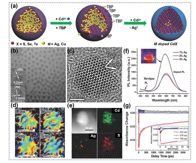
Fig. 5 Synthesis and characterizations of 0D doped TMC materials by CE reactions. a Illustrations showing the synthesis process of M-doped CdX (M = Ag, Cu; X = S, Se, Te) nanocrystals. TBP represents tributylphosphine. b TEM image, c HRTEM images, d strain mapping images and e EDS elemental mapping images of Ag-doped CdS quantum dots (QDs). f Room temperature steady-state fluorescence spectra with different Ag-dopant concentrations, and the inset shows a digital photograph of fluorescence under 365 nm ultraviolet irradiation. PL represents photoluminescence. g Kinetic traces at representative wavelengths are also shown (pump laser wavelength: 390 nm). Reproduced with permission [100]. Copyright 2015, John Wiley and Sons |
2.3.2 Synthesis of 0D TMC Alloys
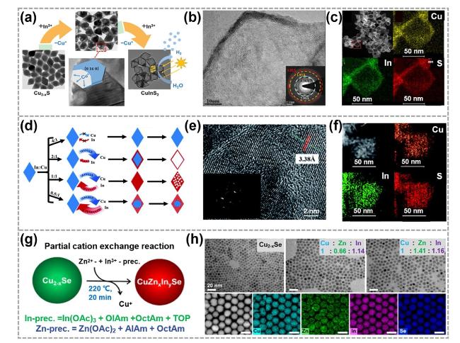
Fig. 6 Synthesis and characterizations of TMC alloys by CE reactions. a TEM images showing the structural evolution from Cu2-xS dodecahedrons to CuInS2 ones. b, c STEM images and corresponding EDS elemental mapping images of CuInS2 dodecahedrons. Reproduced with permission [18]. Copyright 2019, American Chemical Society. d The different products derived from In3+—for—Cu+ CE in Cu7S4 nanocrystals at different In: Cu ratio. e, f HRTEM image and the corresponding EDS elemental mapping images for the product in d with the In: Cu ratio of 1: 1. Reproduced with permission [116]. Copyright 2019, Royal Society of Chemistry. g Illustrations showing the synthesis of CuZnxInySe nanocrystals. h HRTEM images and corresponding EDS elemental mapping images of CuZnxInySe nanocrystals. Reproduced with permission [118]. Copyright 2023, American Chemical Society |
2.3.3 Synthesis of 0D TMC Heterostructures
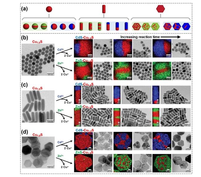
Fig. 7 Synthesis and characterizations of the segmented heterostructures obtained by CE reactions. a Synthesis illustrations of Cu1.8S/CdS and Cu1.8S/ZnS segmented heterostructures. Reproduced with permission [122]. Copyright 2020, American Chemical Society. TEM images and corresponding EDS elemental mapping images of Cu1.8S b spheres, c rods and d hexagonal plates. Reproduced with permission [25]. Copyright 2018, The American Association for the Advancement of Science |
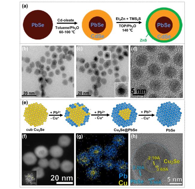
Fig. 8 Synthesis and characterizations of the core-shell heterostructures obtained by CE reactions. a Synthesis illustrations of PbSe@CdSe QDs. Ph2O represents phenyl ether, TOP represents trioctylphosphine, Et2Zn represents diethyl zinc and TMS2S represents hexamethyldisilathiane. b Low-resolution image of 6.1 nm PbSe cores with 1.4 nm CdSe shells. c Low-resolution image of the same area as b, but tilted by 12° to enhance the diffraction contrast. d High-resolution image of PbSe@CdSe QDs, showing a relatively defect-free interface. Reproduced with permission [123]. Copyright 2008, American Chemical Society. e Cu2Se@PbSe heterostructures and f-h corresponding HRTEM images as well as corresponding EDS elemental mapping images. Reproduced with permission [40]. Copyright 2017, American Chemical Society |
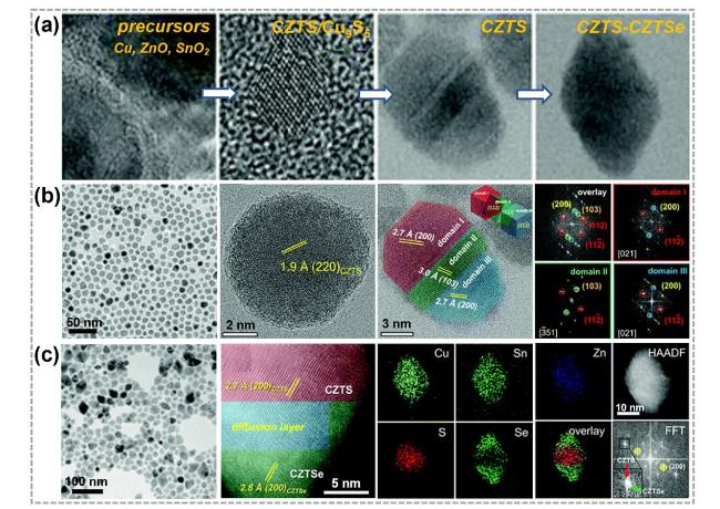
Fig. 9 Synthesis and characterizations of 0D TMC heterostructures obtained by a combining CE and AE strategy. a TEM and HRTEM images of synthesis Cu2ZnSnS4-Cu2ZnSnSe4 (CZTS-CZTSe) nano-heterostructure process. b TEM images of CZTS nanocrystals and fast Fourier transform (FFT) patterns of overlay, domain I (red), domain II (green), and domain III (blue). c TEM and high-resolution scanning TEM (HR-STEM) images of CZTS-CZTSe heterostructures and corresponding STEM-EDS elemental mapping images as well as corresponding FFT pattern of CZTS-CZTSe nanocrystals. Reproduced with permission [128]. Copyright 2021, RSC Pub. (Color figure online) |
3 1D TMCs
3.1 Synthesis of 1D Nanorods
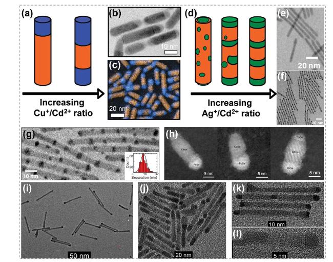
Fig. 10 Synthesis of hetero-nanorods by ion exchange process. a The morphology of CdS-Cu2S nanorods by CE reactions. b, c TEM image and color-composite energy-filtered transmission electron microscopy (EFTEM) image of the obtained CdS-Cu2S nanorods. d Illustration of CdS-Ag2S nanorods produced by CE methods. Reproduced with permission [133]. Copyright 2009, American Chemical of Society. e, f TEM images of the pristine CdS nanorods and obtained CdS-Ag2S nanorods. g TEM images of CdS-Ag2S nanorods with inset showing histogram of Ag2S segment spacing (center-to-center). Reproduced with permission [131]. Copyright 2007, The American Association for the Advancement of Science. h HAADF-STEM image of CdS/Pd4S hybrid nanorods. Reproduced with permission [134]. Copyright 2015, American Chemical Society. i Tip growth of Pd4S on CdS nanorods with a diameter of 5.9 nm. j The extensive growth of Pd4S on CdS nanorods with a broad size distribution. k Close-up of the sample shown in i. l HRTEM of a single CdS-Pd4S nanorod from the sample shown in j. Reproduced with permission [11]. Copyright 2011, John Wiley and Sons |
3.2 Synthesis of 1D Nanowires
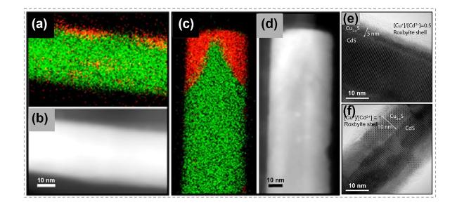
Fig. 11 Synthesis and characterization of CdS@Cu2-xS nanowires by ion exchange process. a-d EDS element mapping images for Cd (in green) and Cu (in red) and corresponding STEM images. a, b Images showing the substitution started at the side surface of nanowires. c, d Images showing the substitution started at the tips of nanowires. e, f HRTEM images of CdS@Cu2-xS core@shell nanowires. e A core@shell nanowire obtained with a 0.5:1 Cu+/Cd2+ ratio, f a core@shell nanowire with increasing shell thickness obtained with a 1:1 Cu+/Cd2+ ratio. Reproduced with permission [129]. Copyright 2014, American Chemical Society. (Color figure online) |
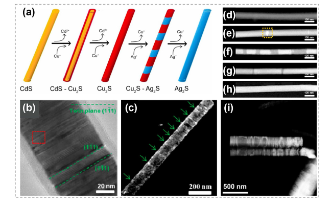
Fig. 12 Synthesis and characterizations of Cu2S-Ag2S heterostructure nanowires. a Illustration shows the formation process of Cu2S-Ag2S superlattice nanowires. b TEM image of a Cu2S nanowire transformed from a CdS nanowire. The twin planes are the (11̅1) planes. c Dark-field TEM image of a single Cu2S nanowire viewed along the [109] zone axis and presented by selecting the (11̅1) diffracted beam. The green arrows indicate locations of the (11̅1) twins. d-h HAADF-STEM images of the Cu2S-Ag2S nanowires formed. Reaction times are d 0 s, e 6 s, f 24 s, g 48 s, h 60 s. i HAADF-STEM image of Ag2S/Cu2S nanowires after CE reactions in monoclinic Cu2S structure. Reproduced with permission [28]. Copyright 2014, American Chemical Society. (Color figure online) |
3.3 Synthesis of 1D Nanotubes
Fig. 13 Synthesis of PtTe2 nanotubes via the shape evolution in Cd+-Pt4+ exchanging process. a TEM image of CdTe nanowires, b TEM image of PtTe2 nanotubes derived from CdTe nanowires through CE reactions. c HRTEM image of a PtTe2 nanotube indexed as the hexagonal phase with lattice spacing of 0.28 nm along the [100] direction. The inset shows the Fourier transformed ring pattern of PtTe2 nanotubes. Reproduced with permission [39]. Copyright 2010, American Chemical Society |
3.4 Synthesis of 1D Nanobelts
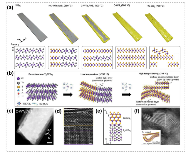
Fig. 14 Structure diagram and characterizations of TMC nanobelts by atomic substitution process. a The temperature-dependent synthesis of nanobelts via the substitution of chalcogen. NC-WTe2/WS2 represents non-curled WTe2/WS2, C-WTe2/WS2 represents curled WTe2/WS2 and C-WS2 represents curled WS2. b Schematic showing controlled conversion process at different temperatures. c HAADF-STEM image (scale bar: 30 nm) of the curled WTe2/WS2 grown at 600 °C. d, e Atomic-Resolution STEM image (scale bar: 1 nm) and atomic configurations showing the interface structure of the curled WTe2/WS2 heterostructure. f Plan-view Atomic-Resolution STEM image (scale bar: 2 nm) and atomic model showing the WS2 layer was deformed. Reproduced with permission [136]. Copyright 2020, John Wiley and Sons |
4 2D TMCs
4.1 Initiation of Atomic Substitution
4.1.1 Vacancy-Initiated Substitution
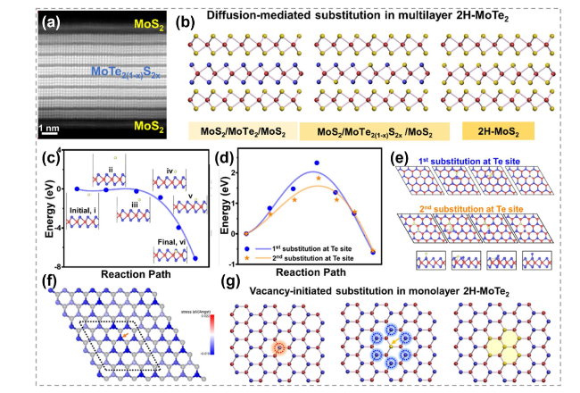
Fig. 15 Mechanism of atomic substitution initiated by vacancies. a Magnification HAADF-STEM cross-sectional image of the sulfurized MoTe2. b Diffusion-mediated substitution mechanism in multilayer MoTe2 (Red: Mo, yellow: S, and blue: Te) c Energy barrier for S substitution at Te vacancy. Insets are the path details. d Energy barriers and e path details for S substitution at Te sites (blue) in the perfect MoTe2 (orange) and after the insertion of first S. f Force map after the replacement of first S. g Diffusion-mediated substitution mechanism in multilayer MoTe2. Reproduced with permission [152]. Copyright 2021, American Chemical Society. (Color figure online) |
4.1.2 Grain Boundary-Initiated Substitution
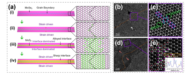
Fig. 16 Mechanism exploration in atomic substitution initiated by grain boundary. a Schematic showing growth of MoS2 channels. b, c Annular dark-field scanning transmission electron microscopy (ADF-STEM) images of intrinsic 60° GB (orange dashed line) within pristine monolayer MoSe2 and atomic arrangement of this GB (blue and purple circles: Mo and Se atoms) resembles that in MoS2 nano-channels. d, e ADF-STEM images showing part of MoSe2-MoS2 hybrid winding channel. The red arrows represent the sulfidation direction. Purple arrows mark 2Se atoms and yellow-purple arrows mark S + Se atoms, with line intensity profile showing in the inset. Reproduced with permission [157]. Copyright 2020, Spring Nature. (Color figure online) |
4.1.3 Edge-Initiated Substitution
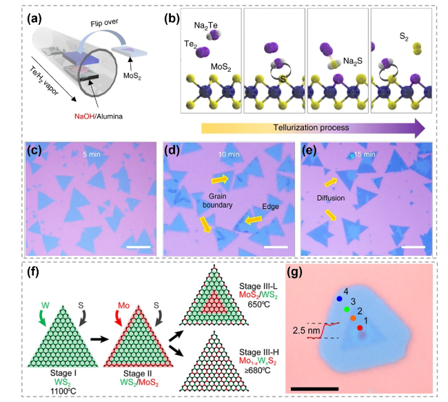
Fig. 17 Mechanism of atomic substitution initiated by edge. a Alkali-metal-assisted transformation from MoS2 to MoTe2. b Schematic showing Na-assisted tellurization process. c-e Optical images showing the evolution from MoS2 to MoTe2. Reproduced with permission [158]. Copyright 2017, Springer Nature. f Illustration showing the substitution of W in WS2 by Mo at different temperatures (W atoms are shown in green, Mo atoms are red, S atoms are black). g Optical image of a typical heterostructure revealing a distinct core-ring structure. Scale bar is 5 μm. Reproduced with permission [159]. Copyright 2016, American Chemical Society. (Color figure online) |
4.2 Synthesis of 2D TMC Binary Compounds
4.2.1 Substitution Between TMCs
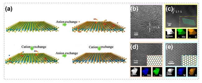
Fig. 18 Transformation between different TMCs by atomic substitution. a Schematic showing ion exchange in TMCs. b HRTEM image of a SnS2 nanosheet before CE reactions. c HRTEM and element mapping images of a MoS2 after CE. d STEM and element mapping images of a MoSe2 after AE. e STEM and element mapping images of a WS2 after CE. Reproduced with permission [27]. Copyright 2017, American Chemical Society |
4.2.2 Oxygen-Chalcogen Substitution
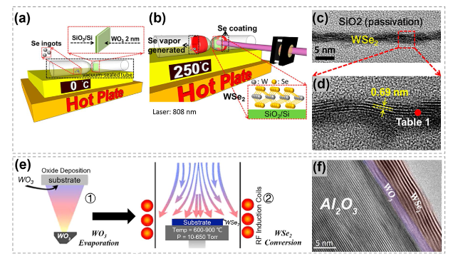
Fig. 19 Synthesis of WSe2 by the oxygen-chalcogen exchange process. a Illustration showing 2 nm-thick WO3 on SiO2/Si and Se ingots was vacuum-sealed together. b Illustration showing the formation of WSe2 when heating up to 250 °C. c Across-sectional TEM image of WSe2. d HMTEM image revealing the interlayer distance of the WSe2. Reproduced with permission [160]. Copyright 2015, American Chemical Society. e Synthesis process of WSe2 converted from amorphous WO3 and hexagonal stabilized WO3 films. Thermal evaporated WO3 films were annealed via rapid thermal annealing and then converted to WSe2 via cold wall furnace. f TEM image of the obtained layered WSe2 structure and the unconverted WO3 film between sapphire and WSe2. Reproduced with permission [164]. Copyright 2015, IOP Publishing |
4.2.3 Iodine-Chalcogen Substitution
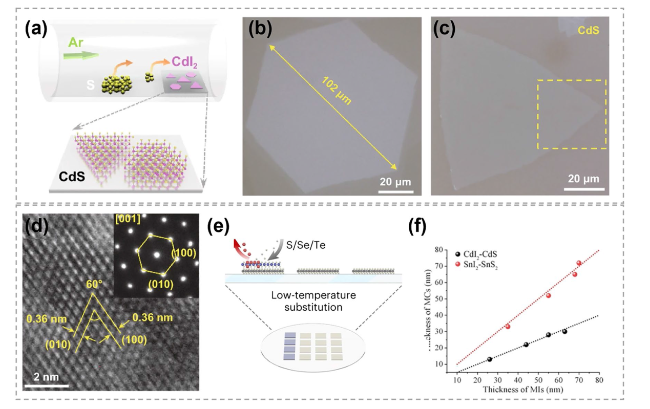
Fig. 20 Chalcogen substituting iodine in the synthesis of TMCs. a Schematic of the substitution and atomic structure of CdS flakes on mica substrate by chemical sulfurization method. b Representative optical microscope images of converted CdI2 thin flake on mica substrates. c Representative optical images of original large-scale CdI2 thin flake and converted CdS thin flake on mica substrates, respectively. d HRTEM image of converted CdS flakes. The inset is the selected area electron diffraction pattern taken along the direction [001] of CdS flakes. Reproduced with permission [35]. Copyright 2021, Springer Nature. e Schematic showing the preparation of CdS flakes on mica substrate by chemical sulfurization method. f The thickness of CdI2 and SnI2 flakes after being converted to CdS and SnS2. Reproduced with permission [34]. Copyright 2023, Springer Nature |
4.2.4 Nitrogen-Chalcogen Substitution
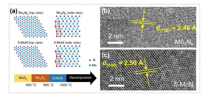
Fig. 21 Synthesis of nitrides by atomic substitution. a Crystal structures of Mo5N6 and δ-MoN. b, c HRTEM images of the obtained Mo5N6 and δ-MoN. Reproduced with permission [165]. Copyright 2022, American Chemical Society |
4.3 Synthesis of 2D TMC Heterostructures
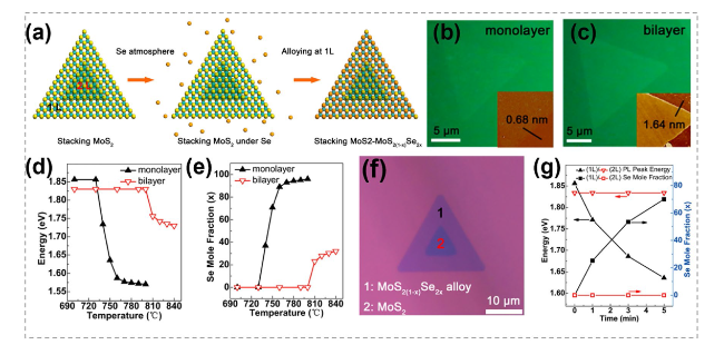
Fig. 22 Heterostructure synthesized by chalcogenides substitution. a Schematic diagram of the preparation of MoS2-MoS2(1-x)Se2x heterostructure by the Se substitution in a designed stacking MoS2 nanosheet. b, c Optical images of monolayer and bilayer MoS2 nanosheets after substitution with the corresponding AFM images shown in inset. d, e Bandgap values and compositions of the two sheets as a function of annealing temperature. f, g Optical image, bandgap values and compositions of the obtained MoS2-MoS2(1-x)Se2x heterostructures. Reproduced with permission [23]. Copyright 2017, American Chemical Society |
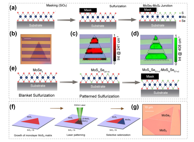
Fig. 23 The selective substitution of TMC heterostructure synthesis. a Schematic showing the heterostructures synthesis protocol based on the sulfurization of patterned MoSe2 monolayers. b Optical image of a representative lateral heterostructure. c, d Mapping intensity of the A1g Raman modes of MoSe2 in (b) at 241 cm-1 and MoS2 at 408 cm-1, respectively. e Schematic showing the realization of an (x, y)-heterostructure with x < y. Reproduced with permission [176]. Copyright 2020, American Chemical Society. f Schematic illustrations showing the formation process of MoS2-MoSe2 by laser patterning and selective selenization. g Microscopy images after the process illustrated in f. Reproduced with permission [177]. Copyright 2021, American Chemical Society |
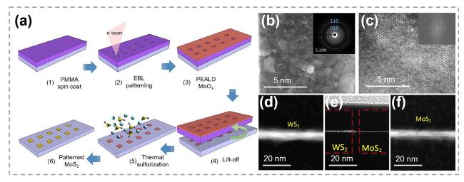
Fig. 24 Patterned synthesis of TMC by substituting oxygen atoms with chalcogens. a Scheme of the atomic layer deposition enabled growth of large area patterned MoS2. b STEM image showing the uniform coverage of the polycrystalline MoS2 film. The inset shows a selective area electron diffraction pattern from the same sample which confirms the polycrystalline. c HR-STEM image of MoS2. d-f Low magnification cross-sectional HR-STEM characterization of e WS2/MoS2 junction and magnified cross-sectional HR-STEM images of d WS2 and f MoS2 regions. Reproduced with permission [178]. Copyright 2020, IOP Publishing |
4.4 Synthesis of 2D TMC Janus Structures
Fig. 25 Synthesis of 2D TMC Janus structures by atomic substitution. Synthesis of 2D TMC Janus structures by atomic substitution. a Schematic illustration of the reaction setup for Janus SMoSe monolayer. b Different views of an eight-unit-cell Janus SMoSe monolayer. c Proposed mechanism for the sulfurization of monolayer MoSe2 at different temperatures. d HRTEM image of the Janus SMoSe lattice. Reproduced with permission [182]. Copyright 2017, American Chemical Society. e Schematic showing the asymmetric MoSSe monolayer structure. f Schematics showing key reaction steps for room-temperature atomic-layer substitution process. g Tilted ADF-STEM image of the Janus MoSSe sample. Reproduced with permission [156]. Copyright 2021, NATL ACAD SCIENCES |
4.5 Synthesis of 2D TMC Alloys
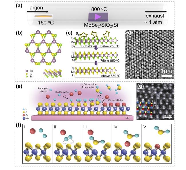
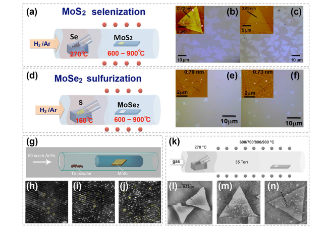
Fig. 26 Synthesis of TMC alloys by atomic substitution. a, d Schematic illustration of the experimental set-up for the selenization/sulfurization process. b, e Optical micrographs for the as-synthesized MoS2/MoSe2. c, f Selenized (sulfurized) MoS2/MoSe2 (at 800 °C) on sapphire substrates. Reproduced with permission [150]. Copyright 2014, Frontiers Media S.A. g Schematic setup for the post-growth substituting. h-j Atomically resolved ADF-STEM images showing the atomic structure of Te-doped MoS2 monolayer at different growth temperature. A number of bright sites corresponding to the local Te sites can be distinguished (marked with yellow circles). Scale bar: 1 nm. Reproduced with permission [151]. Copyright 2018, IOP Publishing. k Schematic illustration for the selenization process. l-n AFM images for the MoS2 flake l before and m after, n selenization at 800 °C. Reproduced with permission [184]. Copyright 2014, John Wiley and Sons |
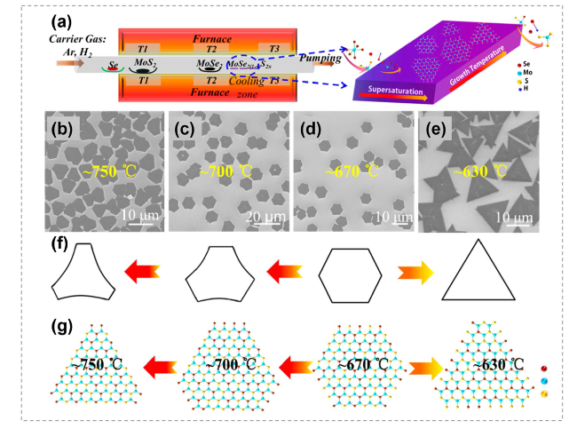
Fig. 27 Controllable synthesis of MoS2(1-x)Se2x alloys by atomic substitution. a Illustration of three-zone furnace setup for MoS2(1-x)Se2x (x = 0.41-1.00) monolayer growth. b-e SEM images of MoS0.78Se1.22 domains obtained at different deposition temperatures. f Schematic illustration of different morphologies at different temperatures. g Atomic structures showing domains obtained at different temperatures. Reproduced with permission [185]. Copyright 2015, American Chemical Society |
4.6 Synthesis of 2D Doped TMC Materials
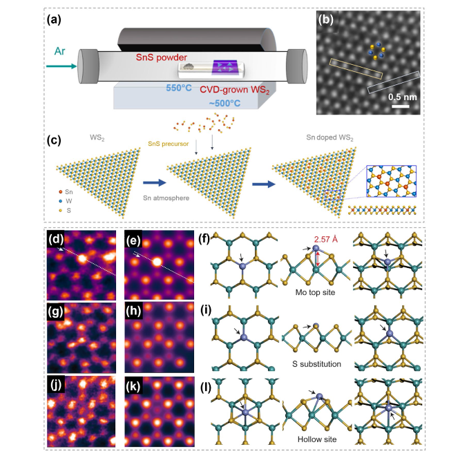
Fig. 28 Metal atoms substitution doping of TMCs. a Schematic showing the thermal doping of Sn in WS2. b ADF-STEM images showing the area of Sn-doped WS2 monolayer. c Schematics showing the formation of Sn-doped WS2 monolayers. Reproduced with permission [155]. Copyright 2019, American Chemical Society. d-f ADF-STEM image, image simulation and atomic model from density functional theory (DFT) geometry optimization of the Co on Mo atop site. g-i HAADF image, image simulation from DFT geometry optimization and atomic model from geometry optimized DFT of a Co-substituted S site. j-l HAADF image, image simulation and atomic model from DFT geometry optimization showing Co in the hollow site. Reproduced with permission [154]. Copyright 2017, Springer Nature |
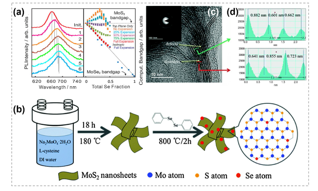
Fig. 29 Chalcogens substitution doping in TMCs. a Normalized room-temperature photoluminescence spectra of a single-layer MoS2 film after sputtering and diselenodiphenyl insertion cycles. Reproduced with permission [188]. Copyright 2014, American Chemical Society. b Schematic illustration of the synthesis procedure for the Se-doped MoS2 nanosheets. c HRTEM image and (inset) the corresponding selected area electron diffraction patterns of Se-doped MoS2 nanosheets. d The lattice distances of the labeled green and red lines in c. Reproduced with permission [189]. Copyright 2015, The Royal Society of Chemistry. (Color figure online) |
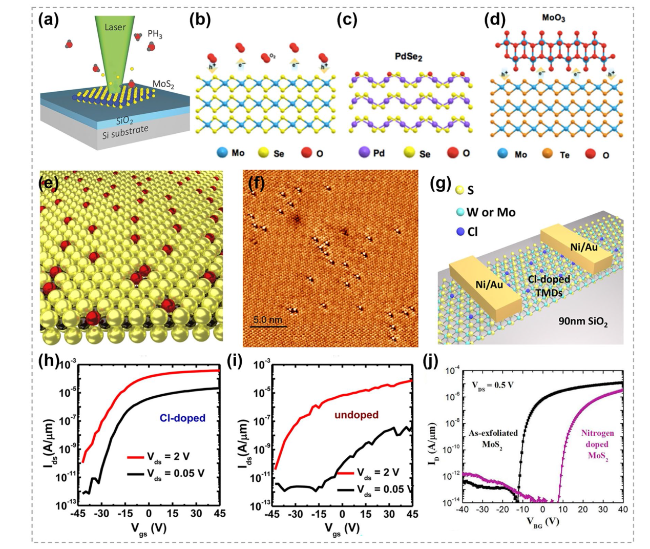
Fig. 30 Nonmetal elements substitution doping in TMCs. a Schematic diagram of the laser-assisted doping method. Reproduced with permission [197]. Copyright 2016, John Wiley and Sons. b Illustration showing charge transfer from oxygen molecules. c Isoelectronic substitution of chalcogen atoms in TMCs. d Illustration showing charge transfer from oxide. Reproduced with permission [198]. Copyright 2020, Springer Nature. e Schematic representation of atmospheric oxygen atoms getting adsorbed on a MoS2 monolayer. f Scanning tunneling microscope image of O atoms (bright spots) absorbed at S vacancies (dark triangles) sites. Reproduced with permission [199]. Copyright 2018, Springer Nature. g Schematic of Cl-doped few-layer WS2 back-gate field-effect transistors (FETs). h Transfer characteristics of the device (Cl-doped). The Ion/Ioff ratio is about 4 × 10⁶ and 3 × 10⁷ at Vds of 2 and 0.05 V, respectively. i Transfer characteristics of the device (undoped). The Ion/Ioff ratio is about 2 × 10⁶ and 1.1 × 10⁴ at Vds of 2 and 0.05 V. Reproduced with permission [194]. Copyright 2014, American Chemical Society. j IDS-VGS characteristics of multilayer nitrogen-doped MoS2 FET. Reproduced with permission [195]. Copyright 2016, American Chemical Society |
5 3D Materials
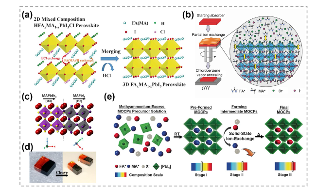
Fig. 31 Atomic substitution in 3D materials. a Schematic diagram showing the transformation of 2D mixed HFAxMA1-xPbI3Cl into 3D FAxMA1-xPbI3 (MA = methylammonium, FA = formamidinium). Reproduced with permission [203]. Copyright 2016, John Wiley and Sons. b Illustration showing the preparation of compositionally graded mixed-cation lead mix-halide perovskite absorbers. Reproduced with permission [204]. Copyright 2018, John Wiley and Sons. c, d Atomic structure and optical images of MAPbBr3/MAPbI3 heterostructures. Reproduced with permission [205]. Copyright 2016, American Chemical Society. e MA-mediation synthesis of FA1−xMAxPbI3 mixed-organic-cation iodide perovskite from MA+-excess precursor solutions. X− denotes an anion that does not conform with the structure. Reproduced with permission [206]. Copyright 2017, John Wiley and Sons |


