HIGHLIGHTS
1 Introduction
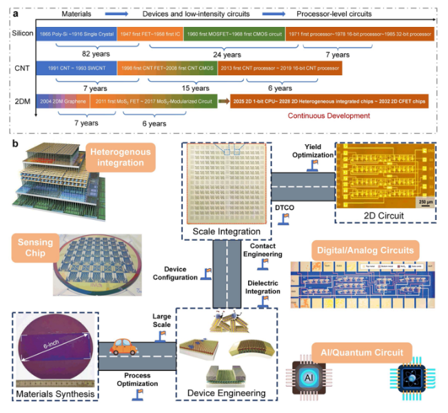
Fig. 1 A schematic diagram of the general roadmap for 2D circuits. a Development timeline of silicon-based, carbon nanotube-based, and 2D ICs. b Route for the realization of 2D circuits and possible applications in the future. Reproduced with permission [17,18,19,20]. Copyright (2017), (2018), (2021), (2022), Springer Nature. Reproduced with permission [21]. Copyright (2023), American Chemical Society. Reproduced with permission [22]. Copyright (2017), Elsevier |
2 Promises of 2D Materials Toward Chips
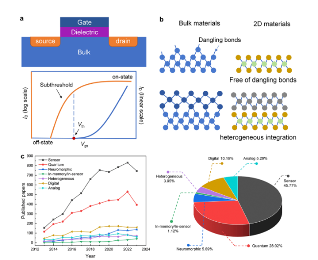
Fig. 2 a Schematic of a traditional FET and typical transfer characteristic of FET device. b Partial advantages of 2D materials over bulk materials. c Number of 2D material publications from 2013 to 2023. (Keywords used for searching “two dimensional materials”, “wafer-scale OR circuit OR array” and the corresponding abbreviation for specific applications like “digital”, several typical 2D materials like MoS2 are also listed as keywords. Source: Web of Science Core Collection, accessed on January 3, 2024) |
3 Process Engineering for 2D Chips
3.1 Material Synthesis
3.1.1 Chemical Vapor Deposition
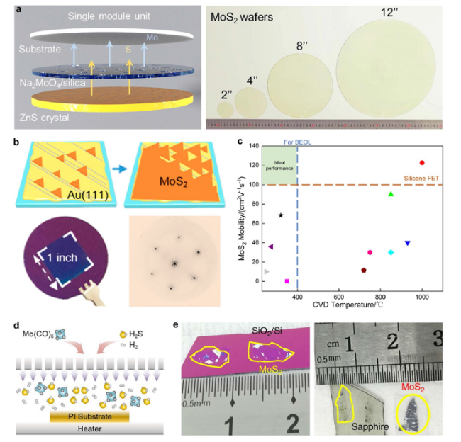
Fig. 3 a Schematic of a single 2-inch producing module unit and photograph of uniform MoS2 film with wafer sizes ranging from 2-, 4-, 8- to 12-inch. Reproduced with permission [42]. Copyright (2023), Science China Press. b Schematic illustration of the MoS2 growth process on Au (111) substrate and representative μ-LEED pattern and photograph of a 1-inch uniform single-crystal MoS2 monolayer. Reproduced with permission [43]. Copyright (2020), American Chemical Society. c The relation between CVD temperature and MoS2 mobility in several reports [19,44,45,46,47,48,49,50,51,52]. d Schematic illustration of the MOCVD process. Reproduced with permission [44]. Copyright (2021), Wiley-VCH. e Optical images of exfoliated MoS2 on SiO2/Si, sapphire, and plastic film. Reproduced with permission [53]. Copyright (2020), Springer Nature |
3.1.2 Metal-Organic Chemical Vapor Deposition
3.1.3 Mechanical Exfoliation Method
3.1.4 Other Methods
3.2 FET Engineering Approaching the Theoretical Limit
3.2.1 Device Configuration
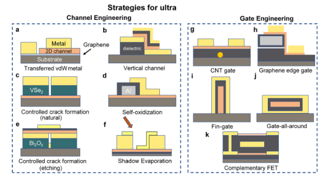
Fig. 4 Typical strategies for ultra-scale transistors. Channel engineering: a Sub-1-nm MoS2 vertical transistors fabricated by transferred vdW metal electrodes [75]. b Ultrashort vertical-channel vdW semiconductor transistors [74]. c Channel defined by controlled crack formation (natural) [72]. d 10 nm short channel transistor fabricated by self-oxidization of aluminum [70]. e Channel defined by controlled crack formation (etching) [73]. f Ultrashort MoS2 transistors fabricated by shadow evaporation [71]. Gate engineering: g buried CNT gate with a diameter of 1nm [33]. h Sidewall graphene edge gate with sub-1-nm thickness [69]. i,j 2D FinFET and GAAFET [77,78]. k Complementary FET comprising p-type WSe2 FET and n-type MoS2 FET [79] |
3.2.2 Dielectric Integration
3.2.3 Contact Engineering
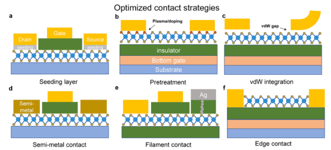
Fig. 5 Typical optimized contact strategies for 2D transistors. a Introduction of a seeding layer for contact integration or improving contact quality [92]. b Doping of contact region or pretreatment of the interface [93]. c VdW integration process [96]. d Development of novel materials such as semi-metal contact [87,97]. e, f Novel contact modes, filament contact, and edge contact [40,98] |
3.3 Material Transfer and Integration
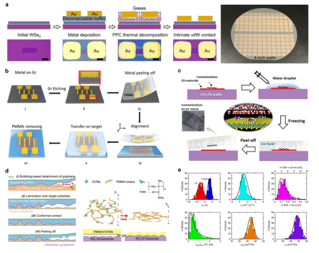
Fig. 6 a Wafer-scale vdW integration processes with four steps and optical images of large-scale vdW contacts. Reproduced with permission [113]. Copyright (2023), Springer Nature. b Schematic illustration of graphene-enhanced vdWs integration. Reproduced with permission [96]. Copyright (2023), Wiley-VCH. c Illustration of the ice-cleaning process. Reproduced with permission [114]. Copyright (2023), Wiley-VCH. d Illustration of techniques and mechanism of the crack-free transfer techniques. Reproduced with permission [115]. Copyright (2022), Springer Nature. e Variability analysis of multiple parameters of hundreds of MoS2 FETs. Reproduced with permission [116]. Copyright (2017), American Chemical Society |
3.4 2D Package
3.4.1 Signal Interconnection
3.4.2 Chip Protection
4 2D Materials for Digital and Analog Chips
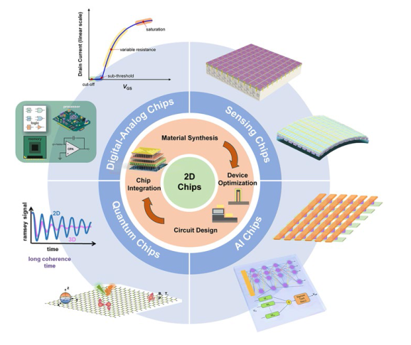
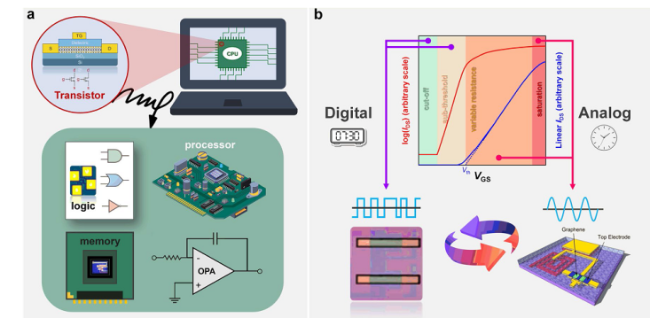
Fig. 7 a Schematic illustration of the enlarged interior of the CPU and applications of transistors, where transistors serve as the dominant functional devices. b Transfer characteristic curve of transistors with four working regions suitable for digital or analog circuits: cutoff, subthreshold, variable resistance, and saturation. X-axis is the gate-source voltage, and y-axis is the drain-source current in logarithmic (left y-axis, red line) and linear (right y-axis, blue line) coordinates |
4.1 2D Digital ICs
4.1.1 Logic Function Realization
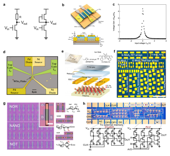
Fig. 8 a Circuit schematic diagram of a resistor-load inverter and NMOS-load inverter. When the NMOS-load inverter works, only one transistor is active, and the upper transistor acts as a resistor. Similarly, the PMOS-load inverter has a similar structure. b Mechanically exfoliated monolayer MoS2 flake (upper) and the schematic illustration of monolayer MoS2 NMOS inverter (bottom). Reproduced with permission [167]. Copyright (2011), American Chemical Society. c Voltage transfer characteristics of a monolayer MoS2 logic inverter with corresponding voltage gain. Reproduced with permission [167]. Copyright (2011), American Chemical Society. d False color optical image of the inverter (scale bar = 4 µm). Reproduced with permission [158]. Copyright (2014), AIP Publishing. e Structure of ambipolar EDLTs with ion-gel thin-film coupling based on monolayer CVD-MoS2 onto a sapphire substrate. Reproduced with permission [159]. Copyright (2016), WILEY‐VCH Verlag GmbH & Co. KGaA, Weinheim. f Optical microscope image of the large-scale chip of MoS2 devices and circuits. The white dashed box is CVD graphene as electrodes and interconnects and the red dashed box is control devices and circuits using Ti/Au electrodes in adjacent. The scale bar is 500 μm. Reproduced with permission [164]. Copyright (2014), American Chemical Society. g Photos of large-area CVD-ReS2 logic circuits after patterning process (scale bar = 500 µm). Reproduced with permission [165]. Copyright (2017), American Chemical Society. h Optical microscope image of 1-bit MoS2 microprocessor with circuit schematics of D-Latch and ALU. The scale bar is 50 µm. Reproduced with permission [20]. Copyright (2017), Springer Nature |
4.1.2 Complex Digital Functional Circuits
4.2 2D Analog ICs
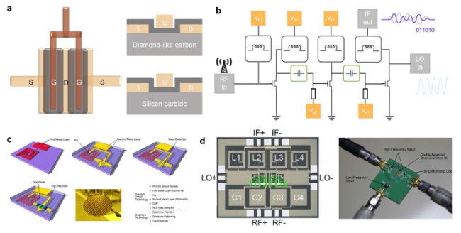
Fig. 9 a Ground-signal-ground (GSG) pad design in dual-channel graphene RF transistor (on the left) and structure diagrams of devices on different substrates (diamond-like carbon & silicon carbide) (on the right). b Schematic diagram of graphene RF receivers including 11 active and passive components. c Schematic diagram of the fabrication process of the graphene IC with the inverted process, a photograph of the 200 mm wafer and the integration flow. Reproduced with permission [180]. Copyright (2015), American Chemical Society. d Optical image of the mixer (on the left) and fabricated double-balanced mixer on PCB (on the right). Reproduced with permission [180]. Copyright (2015), American Chemical Society |
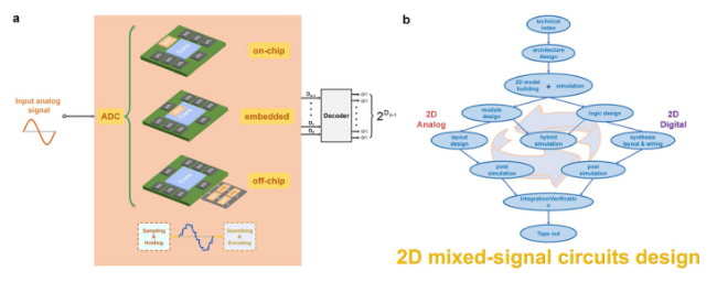
Fig. 10 a Diagram of several connection forms between the core circuit and the ADC converter: on-chip, embedded, off-chip. The analog signal with continuous amplitude is sampled, maintained, quantized and encoded by the ADC converter and then output to the decoder to generate the binary value. b Feasible design process of 2D mixed-signal circuits |
Table 1 Performance metrics of 2D FETs and silicon-based FETs in circuits |
| Parameters | Explanation | 2D material-based FETs1 | Silicon-based FETs2 | |
|---|---|---|---|---|
| Fundamental Indicators | Advanced Indicators | |||
| Ion (mA·μm−1) | $I_{{{\text{DS}}}} = \frac{{W_{{{\text{ch}}}} }}{{2L_{{{\text{ch}}}} }}\mu_{{{\text{FE}}}} C_{{{\text{ox}}}} [2(V_{{{\text{GS}}}} - V_{{{\text{th}}}} )V_{{{\text{DS}}}} - V_{{{\text{DS}}}}^{2} ] ({\text{Linear}}\;{\text{ region}}) I_{{{\text{DS}}}} = \frac{{W_{{{\text{ch}}}} }}{{2L_{{{\text{ch}}}} }}\mu_{{{\text{FE}}}} C_{{{\text{ox}}}} [(V_{{{\text{GS}}}} - V_{{{\text{th}}}} )^{2} ] ({\text{Saturation}}\;{\text{region}})$ | 0.5 (LP), 1 (HP) | 2 (LP), 3 (HP) | 0.6 (LP), 1.5 (HP) |
| VDD (V) | supporting the high level (1) voltage potential for logic gates | 1.4 | 0.5 ~ 0.7 | 0.65 |
| vsat (cm·s−1) | limiting the operating frequency of the device | 0.5 × 10⁷ | 1 × 10⁷ ~ 2 × 10⁷ | 1.6 × 10⁷ |
| Rds(on)3 (Ω·μm) | including RCds, RCss, Rseries metal-semiconductor contact resistance | 400 | 150 ~ 200 | 172 |
| μFE4 (cm2 V−1 s−1) | $\mu_{{{\text{FE}}}} = \frac{{L_{{{\text{ch}}}} g_{m} }}{{W_{{{\text{ch}}}} C_{G} V_{{{\text{DS}}}} }} = \frac{{L_{{{\text{ch}}}} }}{{W_{{{\text{ch}}}} C_{G} V_{{{\text{DS}}}} }} \cdot \left. {\frac{{dI_{{{\text{DS}}}} }}{{dV_{{{\text{GS}}}} }}} \right|_{{V_{{{\text{DS}}}} = {\text{const}}}}$ | 200 | 1000 | 100 |
| SS (mV·dec−1) | ${\text{SS}} = \frac{{{\text{d}}V_{{{\text{GS}}}} }}{{{\text{d}}\lg I_{{{\text{DS}}}} }}$ influencing switching speed | 65 | 60 ~ 62 | 65 |
| fT4 (GHz) | $f_{T} \approx \frac{{g_{m} }}{2\pi }\frac{1}{{(C_{{{\text{GS}}}} + C_{{{\text{GD}}}} )[1 + g_{{{\text{ds}}}} (R_{S} + R_{D} )] + C_{{{\text{GD}}}} g_{m} (R_{S} + R_{D} )}}$ the frequency when the voltage gain is equal to 1, representing the maximum bandwidth that a device is able to achieve | 150 | 350 ~ 450 | 340 |
| fmax5 (GHz) | $f_{\max } = \frac{{f_{T} }}{{\sqrt {4R_{G} (g_{ds} + 2\pi f_{T} C_{{{\text{GD}}}} )} }}$ the frequency when the power gain is equal to 1 | 150 | 400 ~ 500 | 370 |
HP: High Performance. LP: Low Power. VGS, VDS: terminal d.c. voltages. IDS: drain-source current. Wch: channel width. Lch: channel length. Cox: oxide dielectric capacitance. CG: gate capacitance. gm: intrinsic transconductance. CGS: gate-source capacitance. CGD: gate-drain capacitance. gds: drain conductance. RS: source series resistance. RD: drain series resistance. RG: gate resistance. 1The 2D materials here do not specifically refer to one single type of 2D material. Fundamental Indicators: the performance that 2D materials inherently possess and have been reached in the literatures. Advanced Indicators: the performance that have not been realized or is difficult to achieve at present. These two types of indicators are listed as references 2The data of Ion in the “Silicon-based FETs” column derives from the 2021 target in the ITRS 2015 report [188] and the data of radio-frequency performance parameters (fT and fmax) derives from a stacked Si nanosheet [189] 3Rds(on) is the on-state resistance of the FET, including the drain-semiconductor contact resistance (RCds), the source-semiconductor contact resistance (RCss), and the series resistance (Rseries) 4The calculation expressions of μFE and fT are from [190]. In the expression for μFE, CG is the gate capacitance per unit area. 5The calculation expression of fmax is from [191] |
5 Heterogeneously Integrated 2D Devices and ICs
5.1 Heterogeneously Integrated 2D Devices
5.1.1 Complementary Field-Effect Transistor 2D Heterostructure
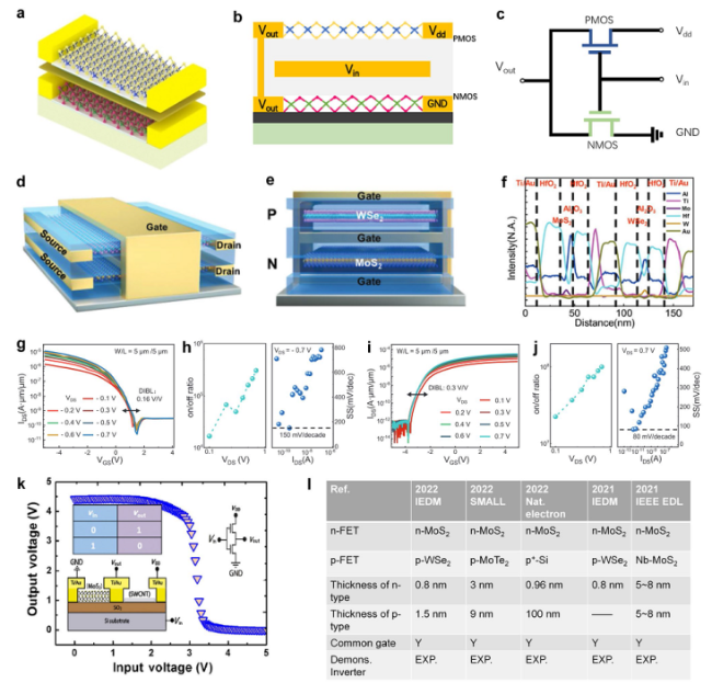
Fig. 11 a Structure schematic of the vertical stacked CFETs. b Structure schematic of the MoS2/WSe2 CFET. c The corresponding equivalent circuit diagram of CFET. d Schematic structure and cross-sectional view of the 2D-CFET device structure. e The top WSe2 FET and bottom MoS2 FET are stacked vertically and share a common gate with a gate-all-around structure. f EDX line scan across the gate-all-around structure (Fig. 11e). g, h Electrical properties of the top WSe2-NS-p-FET in the 2D-CFET. Transfer characteristics at the source-drain voltage from − 0.1 to − 0.7 V. Current on/off ratio versus VDS (left) and SS versus IDS at VDS = − 0.7 V (right). i,j Electrical properties of the top WSe2-NS-p-FET in the 2D-CFET. Transfer characteristics at the source-drain voltage from − 0.1 to − 0.7 V. Current on/off ratio versus VDS (left) and SS versus IDS at VDS = − 0.7 V (right). Reproduced with permission [197] Copyright (2023), John Wiley and Sons. k Output voltage as a function of the input voltage for the MoS2/SWCNT heterogeneous inverters. Reproduced with permission [199] Copyright (2016), Springer Nature. l Comparisons of monolithic 2D CFET devices in previous studies [194,200,201,202,203] |
5.1.2 GAA Nanosheet Vertical-Stacked CFET
5.2 Monolithic Heterogeneously Integrated 2D ICs
5.2.1 Monolithic 2D ICs Heterogeneously Integrated of Low Density
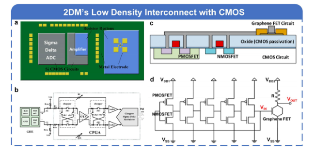
Fig. 12 a Structure design of GHEs with CMOS ICs. b Circuit design of GHEs with CMOS ICs. Reproduced with permission [203]. Copyright (2020), American Chemical Society. c Structure design of integration of 2D FET analog circuit and CMOS digital circuit. d Circuit design of 2D FET analog circuit and CMOS digital circuit. Reproduced with permission [204]. Copyright (2016), American Chemical Society |
5.2.2 Monolithic 2D ICs Heterogeneously Integrated of High Density
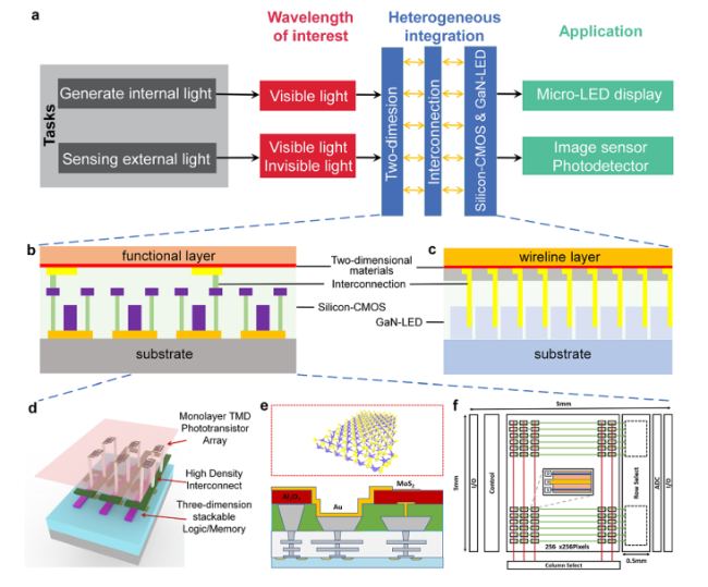
Fig. 13 a Application in photoelectron when using 2D materials. b General heterogeneous integrated structure of sensing external light. c General heterogeneous integrated structure of generating internal light. d Structure of hybrid 3D+IC image sensor. e Structure design of the image sensor. f Circuit design of the image sensor |
6 2D Materials Sensor Chips
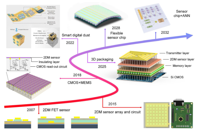
Fig. 14 Developments of 2D material sensors toward chip. After the discovery of graphene, individual 2D material sensors with different gate structure were also demonstrated in 2007. The advent of 2D materials sensor arrays in conjunction with an external processing circuit in 2014 has increased the scale and utility 2D materials of sensors. In 2018, the combination of CMOS and MEMS processes has led to a reduction in the area of 2D materials sensor chips. In 2022, Mei et al. proposed the concept of digital micro-dust to achieve a high-density integrated, low-cost distributed 2D materials sensor chip. Reproduced with permission [222]. Copyright (2022), Elsevier. In 2025, the emerging 3D packaging technology will overturn the distribution structure of sensing networks and open a new era of ultracompact intelligent sensing systems. In 2028, 2D materials sensor chips will evolve toward full flexibility for enhanced sensing capabilities and close cooperation between humans and machines. In 2032, budding sensor technologies integrate sensor networks and advanced algorithms on a chip to reduce the significant power consumption required for transmission and computation |
6.1 Physical Sensors
Table 2 The performance of the physical sensors based on 2D materials |
| Type | Materials | Sensitivity | Time | Range | Integration level | References |
|---|---|---|---|---|---|---|
| Temperature sensor | Graphene | - | - | 283-303 K | Device | [261] |
| Temperature sensor | MoS2 | TCR: ∼1 − 2% K−1 | ~36 μs | 27-85 °C | 4 × 4 array | [267] |
| Thermocouple | Graphene | ΔS: 39 μV K−1 | - | - | On-chip | [262] |
| Temperature sensor | Graphene | |TCR|: ~ 1% K−1 | ~30 ms | 6.6-300 K | On-chip | [265] |
| Pressure sensor | MoS2 | ΔR/R0: 0.011 kPa−1 | 180 ms | 1 − 120 kPa | 8 × 8 array | [270] |
| Pressure sensor | MoS2 | 1.8 MPa−1 (< 500 kPa) | 25/27 ms | 70 Pa to 5 MPa | 20 × 20 array | [271] |
| Pressure sensor | Graphene | 47.8 aF Pa−1 mm−2 | - | 0 − 100 kPa | Sensor chip | [272] |
| Pressure sensor | Graphene | 5.32 × 10⁻⁴ kPa−1 | - | 10 − 100 kPa | MEMS chip | [43] |
| Pressure sensor | Graphene | 5.51 × 10⁻⁵ kPa−1 | - | 0 − 20 MPa | MEMS chip | [273] |
| Strain sensor | Graphene | - | ~ 4/7 ms | 0 − 1.6% | 8 × 8 array | [276] |
| Photodetector | MoS2 | 119.16 A W−1 | 44/41 ms | 405, 532, 638 nm | 8 × 8 array | [279] |
| Photodetector | PtTe2/graphene | ~0.52 A W−1 | ~8.4 μs | 405-1850 nm | wafer-scale | [281] |
| Photodetector | MoS2 | 5.2 × 10⁴ A W−1 | 50 ms | 638, 532, 405, and 852 nm | wafer-scale | [282] |
6.1.1 Temperature Sensors
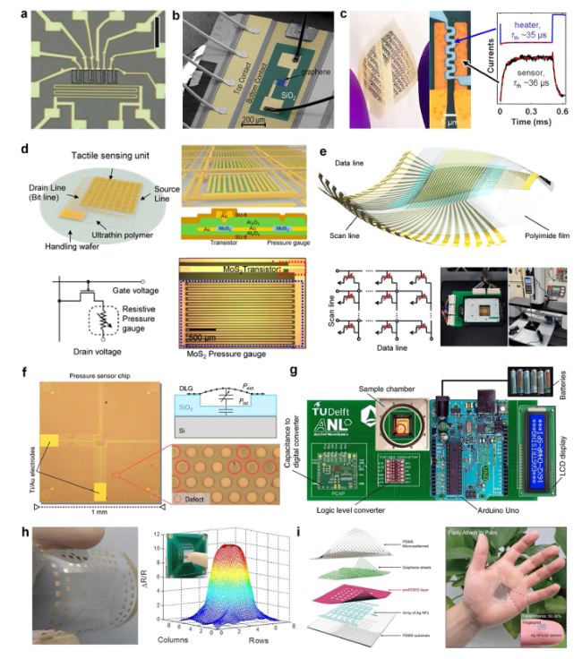
Fig. 15 Temperature, pressure, and strain sensors based on 2D materials. a Optical microscope image of single-material graphene thermocouples showing the measurement configuration. Reproduced with permission [225]. Copyright (2020), Wiley-VCH. b Scanning electron microscopy image of the on-chip integrated graphene thermometer. Reproduced with permission [227]. Copyright (2023), American Chemical Society. c Optical images of the flexible substrate with MoS2 temperature sensor arrays, and sensor response upon pulsed actuation with the heater. Reproduced with permission [228]. Copyright (2022), American Chemical Society. d Schematic illustration of the fully integrated active-matrix MoS2 tactile sensor array, circuit diagram, and optical micrograph of thin-film transistor enabled single pressure gauge unit. Reproduced with permission [229]. Copyright (2019), American Chemical Society. e Active-matrix pressure sensors based on air-dielectric mos2 transistors for wide detection ranges from footsteps to cellular motions. Reproduced with permission [230]. Copyright (2020), American Chemical Society. f Optical image of the sensor chip based on double-layer graphene/PMMA membranes and Ti/Au electrodes. g Readout circuitry PCB board and the red circle indicates the pressure sensor chip. Reproduced with permission [231]. Copyright (2020), Nature Publishing Group. h Optical image of strain sensors with an 8 × 8 device array and measurement of the electric response on applying finger touching. Reproduced with permission [235]. Copyright (2015), American Chemical Society. i Schematic illustration of the structure of pressure sensor arrays based on the photo-reticulated strain localization films, and optical photographs of sensor arrays attached on palm. Reproduced with permission [236]. Copyright (2023), Nature Publishing Group |
6.1.2 Pressure Sensors
6.1.3 Strain Sensors
6.1.4 Optical Sensors
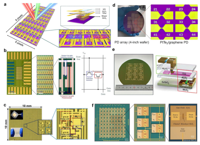
Fig. 16 2D material-based optical sensors. a Schematic illustration of an 8 × 8 image sensor array based on bilayer MoS2 composed of opaque Ti/Au electrodes switching transistor and transparent IZO electrodes phototransistor. b Photograph of the 8 × 8 image sensor array based on bilayer MoS2 and a pixel circuit diagram of proposed image sensor array. Reproduced with permission [238]. Copyright (2020), Nature Publishing Group. c Optical microscopic image and zoom-in image of a fabricated artificial machine vision enhancement MoS2 chip on a sapphire substrate. Reproduced with permission [239]. Copyright (2022), American Association for the Advancement of Science. d Large-scale PtTe2/graphene photodetectors on a 4-inch wafer. Reproduced with permission [240]. Copyright (2022), American Chemical Society. e Wafer-Scale nanoporous MoS2 active-matrix image sensor array on 4-inch Si/SiO2 wafer and cross-sectional view of one pixel. Reproduced with permission [241]. Copyright (2023), Wiley-VCH. f Optical images of the fully integrated 8 × 8 crossbar array of crypto engines, a representative crypto engine with five MoS2 memtransistors, and an individual MoS2 memtransistor. Reproduced with permission [208]. Copyright (2022), Nature Publishing Group |
6.2 Chemical Sensors
6.2.1 Gas Sensors
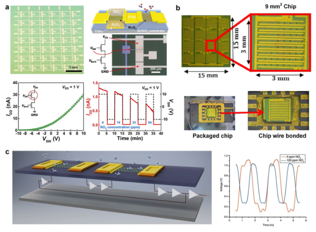
Fig. 17 2D material-based gas sensor. a Morphology and performance of MoS2 TFTs-based gas sensor active-matrix. Reproduced with permission [246]. Copyright (2020), Nature Publishing Group. b Optical images of die, chips and a sensor chip wire bonded into a 16-pin DIL ceramic package. Reproduced with permission [247]. Copyright (2021), IOP Publishing Ltd. c Illustration of CMOS readout circuit and graphene chemiresistive sensor junctions and measured output. Reproduced with permission [248]. Copyright (2017), Nature Publishing Group |
6.2.2 pH Sensors
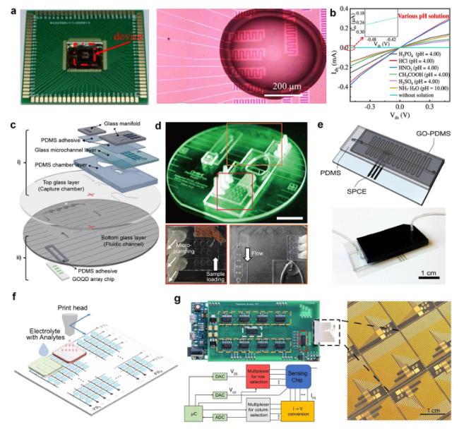
Fig. 18 Ion sensors based on 2D materials. a Optical image of the integrated pH sensors based on MoS2 and the array devices with the added solution. b Selectivity of the integrated pH sensors based on MoS2 for detecting different pH solutions. Reproduced with permission [249]. Copyright (2021), American Chemical Society. c Structural illustration of a multilayered array microdevice based on the solid-phase extraction unit and graphene oxide quantum dot. d Optical image of the assembled microdevice. Reproduced with permission [252]. Copyright (2019), Elsevier. e Scheme and image of LOC device for heavy-metal preconcentration. Reproduced with permission [253]. Copyright (2017), American Chemical Society. f Schematic of the integrated sensor based on graphene transistor arrays. g Optical photograph of the measurement system and the sensor array. Reproduced with permission [254]. Copyright (2022), Nature Publishing Group |
6.2.3 Metal Ion Sensors
6.3 Biological Sensors
6.3.1 Nucleic Acid Sensors
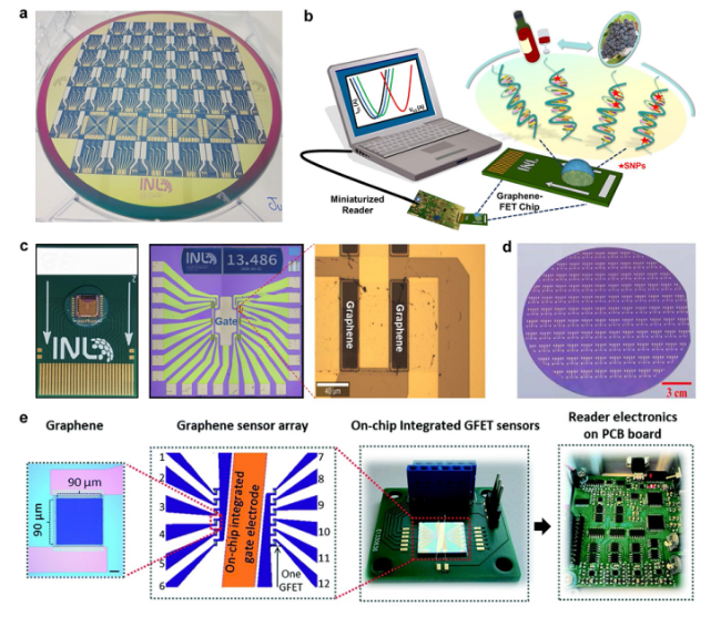
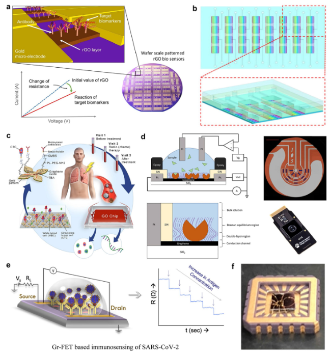
Fig. 19 2D material-based nucleic acid sensors. a Photograph of the 200-mm full wafer with the graphene-based electrochemical chips for the detection of DNA hybridization. Reproduced with permission [22]. Copyright (2018), Elsevier. b Schematic illustration of DNA detection using a portable GFET chip. c Optical image of a ready-to-use GFET chip, layout, and the graphene channel on the chip. Reproduced with permission [258]. Copyright (2023), American Chemical Society. d Optical image of graphene field-effect transistor DNA biosensors fabricated on a 4-inch wafer. Reproduced with permission [259]. Copyright (2022), American Chemical Society. e Image of the graphene sensor array, the integrated on-chip sensor, and the PCB board with reader electronics for COVID-19 detection. Reproduced with permission [260]. Copyright (2022), Royal Society of Chemistry |
6.3.2 Immunological Sensors
Fig. 20 Immunological sensors based on 2D materials. a Schematic of wafer-scale fabricated rGO biosensors for detecting low concentration biomarkers. Reproduced with permission [261]. Copyright (2016), Nature Publishing Group. b Schematic structure of integrated microfluidic biosensing platform based on graphene oxide quantum dots. Reproduced with permission [262]. Copyright (2021), Nature Publishing Group. c Applications of the GO chip within the microfluidic chamber for measuring PD-L1 expression in circulating tumor cells. Reproduced with permission [263]. Copyright (2019), Nature Publishing Group. d Diagram of the foundry fabricated graphene sensor architecture, an entire sensor surface and picture of the complete biosensor. Reproduced with permission [264]. Copyright (2019), Nature Publishing Group. e Schematic of graphene-based field-effect transistor for ultrasensitive immunosensing. f Optical image of graphene-based field-effect transistor after bonding on a ceramic chip carrier. Reproduced with permission [265]. Copyright (2022), American Chemical Society |
6.3.3 Cell-Based Sensors
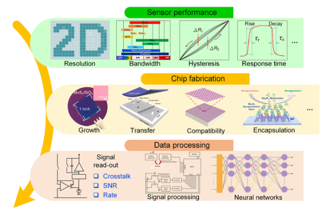
Fig. 21 Overview of key objectives in technology of 2D materials sensors chip. Reproduced with permission [43]. Copyright (2020), American Chemical Society. Reproduced with permission [271,273]. Copyright (2021), (2022), Wiley-VCH. Reproduced with permission [274]. Copyright (2017), Nature Publishing Group |
7 2D AI Chips
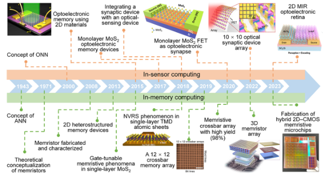
Fig. 22 A roadmap for the evolution of memristor technology and the development of 2D materials for in-memory and in-sensor computing. The past milestones are illustrated [280,281,282,283,284,285,286,287,288,289,290,291,292,293,294,295,296]. Reproduced with permission [285,288,294]. Copyright (2015), (2018), (2022), American Chemical Society. Reproduced with permission [290,292,293,295,296]. Copyright (2019), (2020), (2022), (2023), (2023), Nature Publishing Group |
7.1 2D ICs for In-Memory Computing
7.1.1 2D Material-Based Electrical Synaptic Devices
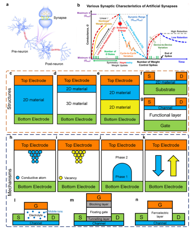
Fig. 23 a Schematic diagram of biological synapses. Reproduced with permission [299]. Copyright (2021), American Chemical Society. b Various synaptic characteristics of artificial synapses. Reproduced with permission [300]. Copyright (2020), American Chemical Society. c-g Different structures of artificial synaptic devices. h-n Several working mechanisms of artificial synaptic devices |
7.1.2 2D Material-Based Electrical Synaptic Arrays
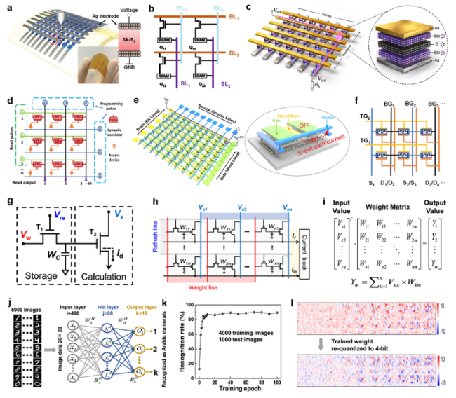
Fig. 24 a Schematic plot of the fully printed Ag/MoS2/Ag memristor in a 4 × 4 crossbar structure on flexible polyimide substrate. Reproduced with permission [331]. Copyright (2019), Wiley-VCH. b An array architecture for matrix-vector multiplication with 1T1R cells to reduce sneak current. c Schematic picture of the van der Waals heterostructure in the crossbar memory array architecture, differing from the traditional one-selector one-resistor and complementary RS. Reproduced with permission [290]. Copyright (2019), Nature Publishing Group. d Circuits of a synaptic transistor-based crossbar array for matrix operations. e 3D schematic illustration of a 10 × 10 MoS2 memtransistor crossbar array. Reproduced with permission [305]. Copyright (2021), American Chemical Society. f Diagram of the dual-gated memtransistor crossbar array. g Circuit schematic of a 2T-1C cell containing storage and calculation modules. h Circuit diagram of the proposed 2T-1C cell array. i A typical diagram of a matrix convolution operation. j Neuromorphic network with three layers, each containing 400 input neurons, 20 hidden neurons, and 10 output neurons. k Recognition rate as a function of training epoch (0-100), using 4,000 images for training and 1,000 images for testing. l Color map showing trained weights are re-quantized to 4-bits. The size of the colormap is 20 × 200. Reproduced with permission [333]. Copyright (2021), Nature Publishing Group |
7.2 2D ICs for In-Sensor Computing
7.2.1 2D Material-based Optoelectronic Synaptic Devices
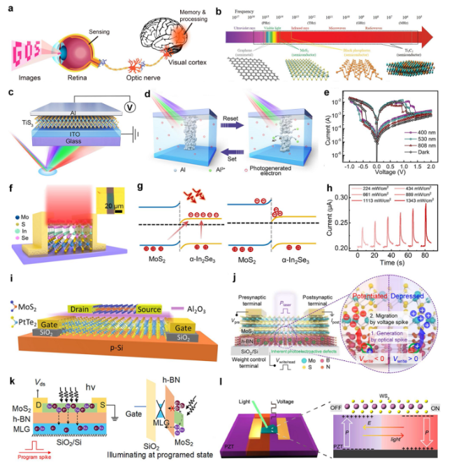
Fig. 25 a Schematic of the human visual system for image sensing, memory, and processing. Reproduced with permission [349]. Copyright (2021), American Chemical Society. b Possible spectral ranges and atomic structures of graphene, MoS2, BP, and Ti3C2. Reproduced with permission [344]. Copyright (2020), Wiley-VCH. c Schematic diagram and d working mechanism of a 2D TiS3-based two-terminal optoelectronic synaptic device with a vertical form. e I − V curves collected under dark conditions and exposed to light of three different wavelengths of the TiS3-based optoelectronic synaptic device. Reproduced with permission [299]. Copyright (2021), American Chemical Society. f Schematic diagram and g band alignment of a In2Se3/MoS2 heterostructure-based two-terminal optoelectronic synaptic device with a planar form. h Modulation of light intensity on the performance of In2Se3/MoS2 devices. Reproduced with permission [294]. Copyright (2022), American Chemical Society. i Schematic diagram of a three-terminal optoelectronic synaptic device based on interfacial carrier capture, with PtTe2/Si as the gate and MoS2 as the channel. Reproduced with permission [343]. Copyright (2022), American Chemical Society. j Schematic diagram of a three-terminal optoelectronic synaptic device based on the MoS2/h-BN heterostructure, in which inherent defects in the material play a key role. Reproduced with permission [345]. Copyright (2021), Nature Publishing Group. k Schematic diagram of a floating-gate optoelectronic synaptic device based on a multilayer graphene/h-BN/MoS2 vertical vdW heterostructure. Reproduced with permission [346]. Copyright (2022), Wiley-VCH. l Schematic diagram of a ferroelectric memtransistor made of a WS2 channel and a ferroelectric PZT thin film for optoelectronic synaptic devices. Reproduced with permission [348]. Copyright (2020), American Chemical Society |
7.2.2 2D Material-Based Optoelectronic Synaptic Arrays
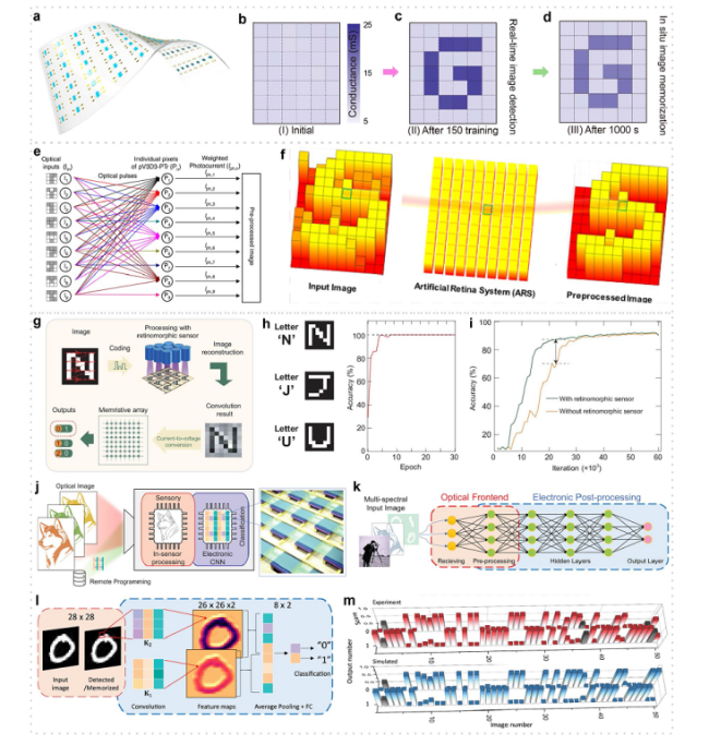
Fig. 26 a Schematic of the optical synapse array fabricated on a flexible PET substrate. b − d Conductance map of a 7 × 6 optical synapse array. Reproduced with permission [349]. Copyright (2021), American Chemical Society. e Schematic diagram showing the image acquisition and neuromorphic data preprocessing by using a 3 × 3 pV3D3-PTr array. Reproduced with permission [351]. Copyright (2020), Nature Publishing Group. f Artificial retina with an array employing 100 (10 × 10) cells to realize the pretreatment. Reproduced with permission [338]. Copyright (2022), American Chemical Society. g Flow chart schematically illustrates the image sensing and processing by the retinomorphic sensor and image recognition by the memristive crossbar. h Image recognition by the neuromorphic vision system. i Comparison of recognition accuracy with and without the retinomorphic sensor. Reproduced with permission [352]. Copyright (2020), Oxford University Press. j bP-PPT array is capable of multispectral infrared imaging and is programmable for in-sensor computing. k bP-PPT array receives images in multiple wavelength bands. l A CNN model for classifying handwriting numbers “0” and “1” from the MNIST dataset. m Experimental results (top, red) for image recognition using the bP-PPT array are compared with the simulation results (bottom, blue). Each bar is the score indicating the possibility of the CNN recognizing an image in the MNIST image library. The incorrectly recognized cases are in gray. Reproduced with permission [353]. Copyright (2022), Nature Publishing Group |
8 2D Quantum Devices and Circuit
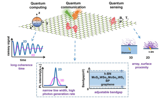
Fig. 27 The application and advantages of 2D materials in quantum information technology, mainly focusing on quantum computing (long coherence time), quantum communication (narrow line width, high photon generation rate, adjustable bandgap) and quantum sensing (array, surface proximity) |
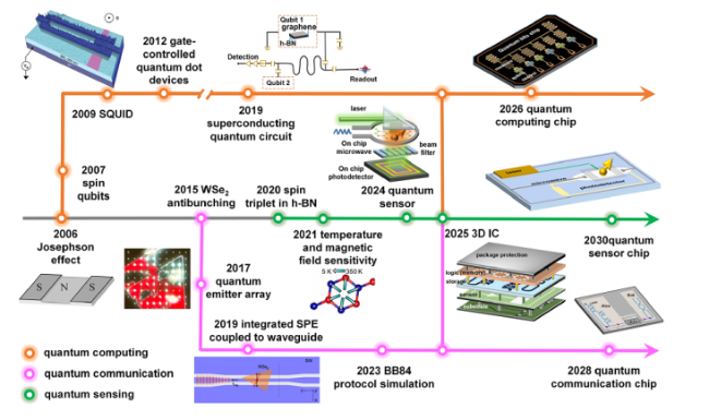
Fig. 28 Diagram of key nodes in the development of 2D materials in quantum computing [354,355,356,357,358], quantum communication [359,360,361,362], and quantum sensing [363,364]. The overall development is from phenomenon discovery to device manufacturing, and then to circuit formation. With the development of 3D integration, chips will eventually be formed. Reproduced with permission [356]. Copyright (2009), American Chemical Society. Reproduced with permission [360,361,364]. Copyright (2017), (2019), (2021), Nature Publishing Group |
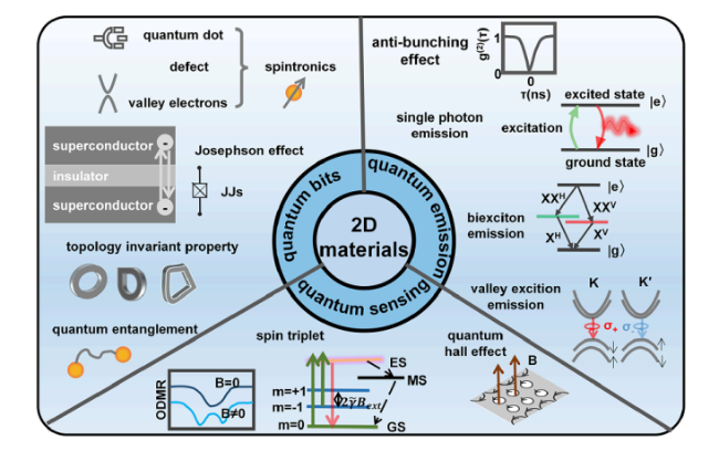
Fig. 29 Quantum phenomena related to quantum bits, quantum emission, and quantum sensing in 2D materials |
8.1 Quantum Effect
8.1.1 Quantum Bits
8.1.2 Quantum Emission
8.1.3 Quantum Sensing
8.2 Quantum Devices
8.2.1 Josephson Junctions
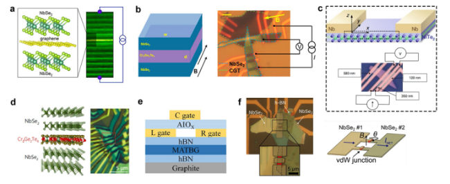
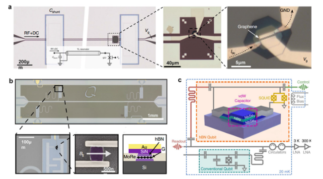
Fig. 30 Development of JJs in 2D materials. a Vertically stacked NbSE2-graphene-NbSE2 JJ: Atomic structure schematic of heterostructure and scanning transmission electron microscope (STEM) image of vertical cross-section. Reproduced with permission [397]. Copyright (2017), American Chemical Society. b π JJs composed of the plane NbSe2/Cr2Ge2Te6/NbSe2. The thickness of the barrier layer is d and the width is w. Optical micrographs and measurement circuit diagrams are shown on the right. Reproduced with permission [398]. Copyright (2022), American Chemical Society. c Schematic diagram of the NiTe2 Josephson diode device and optical microscope image of several JJ devices formed on a single NiTe2 peel sheet. Reproduced with permission [399]. Copyright (2022), Nature Publishing Group. d Josephson coupling of NbSe2/Cr2Ge2Te6/NbSe2 vdW junctions. Left: Atomic diagram of a JJ. Right: Optical micrograph. Reproduced with permission [396]. Copyright (2021), Nature Publishing Group. e A schematic diagram of the interface of gated magic Angle graphene to achieve tunable JJs knots. The MATBG is tuned to a superconducting state utilizing a graphite base gate electrode and the left (L) and right (R) top gate electrodes, and the center (C) gate is tuned locally to a non-superconducting state. The insulated h-BN separates the gate electrodes from the MATBG, and the alumina (AlOx) layer isolates the top upper and lower doors [400]. f SQUID based on twisted NbSe2-NbSe2 JJs. Left: Optical image of an etched SQUID structure. The overlap between the two NbSe2 flakes is highlighted in red in the illustration. Right: Schematic diagram of a SQUID device shown. Reproduced with permission [402]. Copyright (2021), American Chemical Society |
8.2.2 Gate-Controlled Quantum Dots
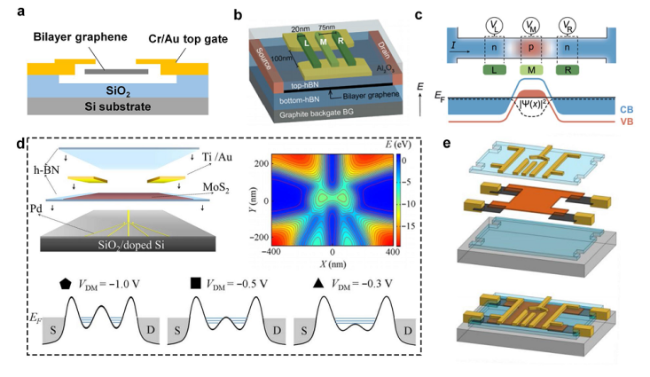
Fig. 31 Development of grid-controlled quantum dots in 2D materials. a Schematic diagram of gate defining a double-layer graphene quantum dot. Graphene is suspended in electrodes. The electric field and carrier density distributions are controlled by the rear and top grid voltages Vb and Vt, while transport measurements can be made by applying a biased Vsd to the electrode [357]. b Schematic diagram of gated BLG quantum dots with adjustable polarity. Where, yellow is the split grid and green is the finger grid L, M and R. Make edge contacts (orange) at both ends of the channel [404]. c Figure shows the adjustable polarity and band diagram. Reproduced with permission [404]. Copyright (2021), American Chemical Society. d h-BN encapsulated grid-controlled MoS2 double quantum dots. Above: Schematic diagram of the sample structure on the left, the potential distribution of COMSOL simulated MoS2 layer on the right, and the closed contour representing the possible location of the quantum dot. Below: Band structure of MoS2 under different gated voltages. This realizes the evolution of a two-quantum-dot system from weak coupling to strong coupling to form a large single quantum-dot. Reproduced with permission [407]. Copyright (2017), American Association for the Advancement of Science. e h-BN/InSe/h-BN heterostructure has graphene contacts and multiple top grids. Each layer structure display: 2D InSe (red), graphene (dark gray), h-BN (blue), Cr/Au contacts, top grid (yellow), Si/SiO2 substrate (light gray). Reproduced with permission [408]. Copyright (2018), American Chemical Society |
8.2.3 Single-Photon Source
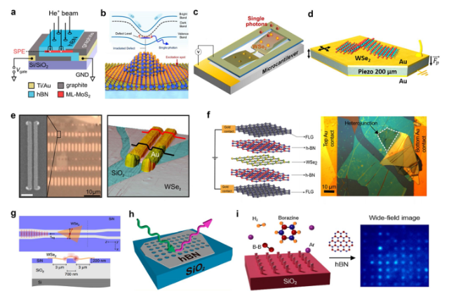
Fig. 32 Development of single-photon sources in 2D materials. a A single-photon emitter matrix is selectively generated in a MoS2 vdW heterogeneous device. Reproduced with permission [411]. Copyright (2021), American Chemical Society. b A single-photon emitter with WSe2 based on nanoscale strain and electron beam irradiation defects shows a strain map of WSe2 on a silica nanocolumn (W atom in blue and Se in yellow). Reproduced with permission [412]. Copyright (2021), Nature Publishing Group. c A single layer WSe2 single-photon emitter on an electrostatically driven microcantilever with a nanopyramid pattern. Reproduced with permission [413]. Copyright (2019), American Chemical Society. d Schematic diagram of a 2D-semiconductor-piezoelectric hybrid driven single-photon emitter with integrated monolayer folds WSe2. Reproduced with permission [414]. Copyright (2019), American Chemical Society. e Plasma waveguide is coupled with the single-photon emitter to enhance the emission. Reproduced with permission [415]. Copyright (2018), American Chemical Society. f Quantum constrained stark effect tuning of a local emitter on a monolayer WSe2 edge. Reproduced with permission [417]. Copyright (2017), American Chemical Society. g Top view and cross section of the integrated WSe2 quantum emitter: WSe2 sheet is integrated on a 220 nm thick single-mode SiN waveguide separated from the body SiN by two air grooves. Reproduced with permission [361]. Copyright (2019), Nature Publishing Group. h h-BN quantum emission array based on edge effect. Reproduced with permission [418]. Copyright (2019), American Chemical Society. i h-BN single-photon emission arrays on nanocolumns. Reproduced with permission [419]. Copyright (2021), American Chemical Society |
8.2.4 Solid-state Quantum Sensors
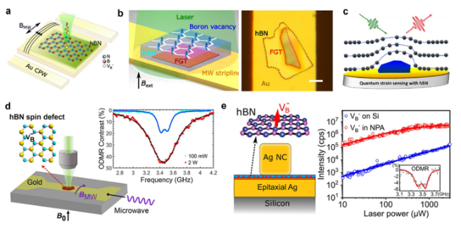
Fig. 33 Development of quantum sensors in 2D materials. a Schematic diagram of spin activity transition detection device for VB− defects in h-BN. The spin states are manipulated by laser and microwave fields. The fluorescence spectra were collected and the spin states were read from the ODMR signal. Reproduced with permission [422]. Copyright (2022), Nature Publishing Group. b Nanoscale quantum imaging of low-dimensional Fe3GeTe2 (FGT) with ferromagnetism by spin defects in h-BN. Reproduced with permission [423]. Copyright (2022), Nature Publishing Group. c Strain quantum sensing of VB− defects in h-BN. Reproduced with permission [425]. Copyright (2022), American Chemical Society. d Photoluminescence enhancement of h-BN spin defects by a gold film microwave waveguide. Its ODMR contrast is up to 46%. Reproduced with permission [427]. Copyright (2021), American Chemical Society. e High resolution magnetic field sensor based on low-loss nano-patch antenna (NPAs) to enhance VB− defect photon emission. An overall strength increase of up to 250 times was observed. Reproduced with permission [428]. Copyright (2022), American Chemical Society |
8.3 Quantum Circuit
Fig. 34 a A superconducting quantum circuit based on a conventional aluminum-based JJ and a parallel plate capacitor combination consisting of superconducting niobium selenide and insulated h-BN crystal layers. The transmitter capacitor is coupled to the read resonator (red) and the drive line (green). Reproduced with permission [432]. Copyright (2018), Nature Publishing Group. b A hybrid superconducting circuit based on S-G-S JJ. Reproduced with permission [431]. Copyright (2018), Nature Publishing Group. c Monolayers of graphene Josephson are incorporated into microwave-frequency superconducting circuits to create graphene-based transporters. Reproduced with permission [433]. Copyright (2021), American Chemical Society |
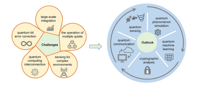
Fig. 35 Challenges (large-scale integration, the operation of multiple qubits, quantum bit error correction, quantum computing interconnection, sensing for complex environments) and outlook (quantum phenomenon simulation, quantum machine learning, quantum communication, quantum sensing, cryptographic analysis) of 2D materials in quantum technology |


