HIGHLIGHTS
1 Introduction
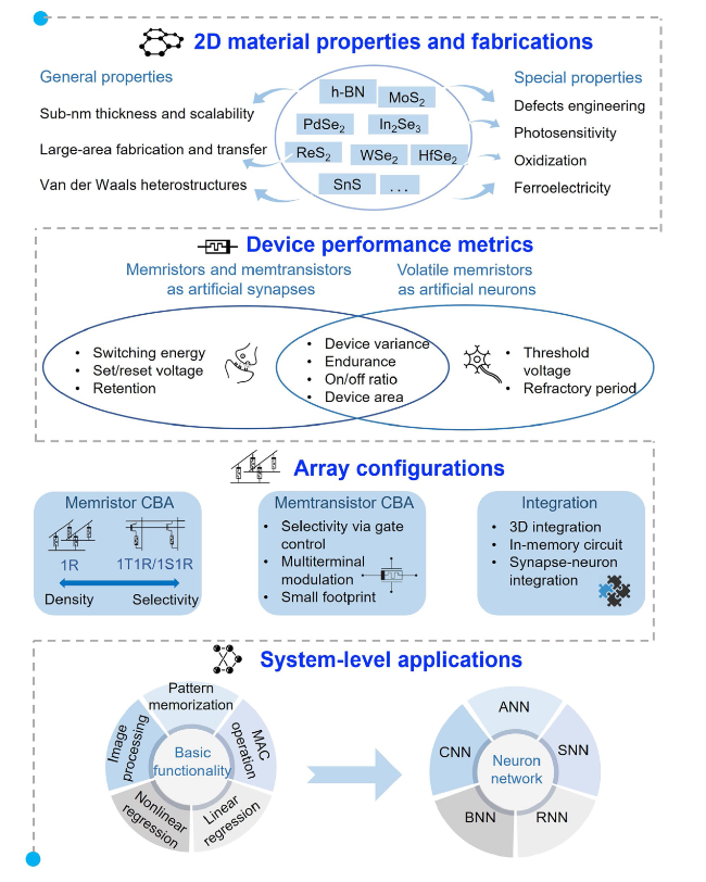
Fig. 1 A schematic of critical steps in 2D material-based in-memory computing applications. First, unique 2D material properties and the fundamental memristive device fabrication and switching mechanisms. Second, different device performance requirements for various applications, including artificial synapses and neurons. Third, different array configurations for integration design, including memristor and memtransistor crossbar array and 3D integration. Last, system-level evaluation of in-memory computing hardware, consisting of the basic computation functionalities and the overall neural network performance |
2 2D Material Platforms for Memristive Device Array Fabrication
2.1 Conductive Filament Formation: h-BN, MoS2, PdSe2 HfSe2 and BP
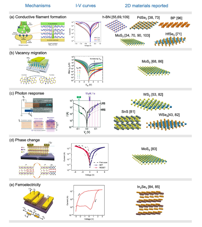
Fig. 2 2D material platforms for memristors and memtransistors with different switching mechanisms: a conductive filament formation, b vacancy migration, c photon response, d phase change and e ferroelectricity. The first column shows the schematic representation of the respective resistive switching mechanisms, the second column displays the measured I-V curves and the final column presents the atomic structures of 2D materials that have been used for crossbar array fabrication. a Reproduced with permission [73], copyright © 2021 Springer Nature Limited. b Reproduced with permission [77], copyright © 2019 WILEY‐VCH Verlag GmbH & Co. KGaA, Weinheim. c Reproduced with permission [82], copyright © 2022 Wiley‐VCH GmbH. d Reproduced with permission [83], copyright © 2018 Springer Nature Limited. e Reproduced with permission [85], copyright © 2022 Wiley‐VCH GmbH |
2.2 Vacancy Migration: MoS2 and ReS2
2.3 Photon Response: WSe2, WS2, and SnS
2.4 Phase Change: MoS2
2.5 Ferroelectricity: In2Se3
3 2D Material-Based Device Performance Metrics
3.1 Performance of Memristive Devices as Artificial Synapse
Table 1 The performance metrics of 2D material-based memristors and memtransistors that have been fabricated with crossbar array |
| Functional 2D material | Switching mechanism | Type | Fabrication method | Device dimension (µm × µm) | Array size | Yield (Working device/tested device) | Programming energy | Switching ratio | Cycle-to-Cycle variation (Total cycles) | Device-to-Device variation of SET voltage | Endurance | Retention (s) | Refs |
|---|---|---|---|---|---|---|---|---|---|---|---|---|---|
| h-BN | Conductive filament formation | Memristor | CVD | 3 × 3 | 10 × 10 | 98% (102/104) | NA | 102 ~ 106 | 1.53% (120) | 5.74% (out of 16 devices) | 120 cycles (DC sweep) | 104 | [55] |
| h-BN | Conductive filament formation | Memristor | CVD | 0.15 × 0.15 | 10 × 10 | NA | 20 fJ | ~ 500 | 13.1% (80) | 28.9% (out of 6 devices) | 8 × 10⁴ (PVS* visible) | Volatile | [55] |
| h-BN | Conductive filament formation | Memristor | CVD | 3 × 3 | 2 × 1 | NA | 125 fJ | 102 | NA | NA | 102 cycles (DC sweep) | 102 | [69] |
| h-BN | Conductive filament formation | Memristor | CVD | 3 × 3 and 0.32 × 0.42 | 4 × 4 and 100 × 100 | Monolayer: 5% (5/100) Multi-layer: 98% (98/100) | NA | ~ 102 | NA | NA | ~ 60 cycles (DC sweep) | NA | [107] |
| PdSexO2-x | Conductive filament formation | Memristor | Exfoliation | 3 × 3 | 3 × 6 | 100% (18/18) | 0.9 pJ | 103 | 3.6% (100) | NA | 7 × 10² cycles (DC sweep) | 105 | [38] |
| PdSe2 | Conductive filament formation | Memristor | Exfoliation | 3 × 3 | 5 × 5 | 100% (25/25) | 11.25 pJ | 102 | ~ 6% (100) | NA | 102 cycles (DC sweep) | 105 | [73] |
| BP | Conductive filament formation | Memristor | Exfoliation | 0.1 × 0.1 | 10 × 10 | NA | NA | 107 | NA | NA | 102 cycles (DC sweep) | 104 | [96] |
| MoS2 | Conductive filament formation | Memristor | Printing | 0.6 × 0.3 | 4 × 4 | NA | 4.5fJ | 107 | NA | NA | 102 cycles (DC sweep) | 4 × 10⁴ | [34] |
| MoS2 | Conductive filament formation | Memristor | CVD | NA | 4 × 4 | NA | NA | 5 ~ 6 | NA | NA | 5 × 10² cycles (DC sweep) | 104 | [70] |
| MoS2 | Conductive filament formation | Memristor | MBE | 5 × 5 and 0.1 × 0.1 | 10 × 10 | NA | 140 pJ | ~ 160 | 18.1% (200) | 18.5% (out of 73 devices) | 107 (PVS blind) | 105 | [90] |
| MoS2 | Conductive filament formation | Memristor | Exfoliation | NA | Synapse 4 × 2 Neurons: 2 | NA | 65 nJ | 103 | NA | NA | 50 cycles (DC sweep) | NA | [103] |
| HfSe2 | Conductive filament formation | Memristor | Solution process | 3 × 3 | 3 × 3 | NA | 0.8 pJ | ~ 150 | NA | NA | 5 × 10² (PVS visible) | 104 | [71] |
| MoS2 | Vacancy migration | Memtransistor | CVD | length < 1 µm | 10 × 10 | 90% (9/10) | 2 pJ to 2 nJ (via gate) | 103 | NA | NA | ~ 8.5 × 10² (DC sweep) | 105 | [68] |
| MoS2 | Vacancy migration | Memtransistor | CVD | 0.4 × 20 | 10 × 10 | 64% (64/100) | 20 fJ | ~ 50 | 5.9% (150) | 11.4% (out of 64 devices) | 150 cycles (DC sweep) | 104 | [86] |
| WS2 | Photon response | Memtransistor | CVD | 1 × 1 | 6 × 6 | NA | 14 pJ | 50-200 | NA | NA | 102 cycles (DC sweep) | 8 × 10⁴ | [82] |
| SnS | Photon response | Memristor | Exfoliation | length ~ 2 µm | 5 × 1 | 100% (5/5) | NA | NA | NA | NA | NA | NA | [81] |
| MoS2 | Phase change | Memristor | Exfoliation | ~ 20 × 20 | 4 × 1 | NA | NA | 102 | NA | NA | 4 × 10⁴ (PVS) | 7 × 10³ | [83] |
| α-In2Se3 | Ferroelectricity | FeFET* | Exfoliation | 4 × 4 | 100 × 1 | NA | 10 fJ | 106 | NA | NA | 104 cycles (DC sweep) | volatile | [84] |
| α-In2Se3 | Ferroelectricity | FeFET | Exfoliation | NA | 2 × 1 × 2(2 layers) | NA | NA | NA | NA | NA | NA | NA | [85] |
*PVS: pulsed voltage stress *FeFET: Ferroelectric field-effect transistor |
3.1.1 Programming Energy
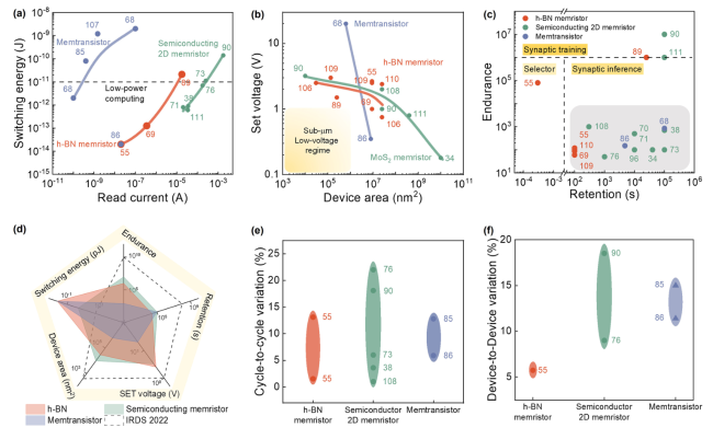
Fig. 3 The summary of memristive device performance. a Switching energy comparison among insulating 2D h-BN-based memristors, semiconducting 2D material-based memristors, and memtransistors. b The relationship between device program voltage and the device size. c The reported device endurance and retention and their suitable working scenarios. d Radar plot of the key merits of the memristive device and the comparison with International Roadmap for Devices and Systems (IRDS) requirements. e Typical cycle-to-cycle variation of 2D material-based memristive devices. f Typical device-to-device variation of 2D material-based memristive devices. The numbers in figures correspond to the number in reference list [34,38,55,68,69,70,71,73,76,85,86,89,90,96,107,109,110,111,112,113] |
3.1.2 Program Voltage and Device Area
3.1.3 Endurance and Retention
3.1.4 Device-to-Device Variation and Cycle-to-Cycle Variation
3.2 Performance of Volatile Memristors as Artificial Neuron
Table 2 Performance metrics of 2D material-based artificial neurons based on volatile memristors |
| Functional 2D material | Type | Fabrication method | Device dimension (µm2) | Mechanism | Threshold voltage (V) | Switching ratio | Endurance | Refs |
|---|---|---|---|---|---|---|---|---|
| MoS2 | Memristor | CVD | 4 | Conductive filamentary formation | 0.35 ~ 0.4 | 106 | 5 × 10⁶ (PVS) | [117] |
| MoS2 | Memristor | CVD | ~ 1 | Conductive filamentary formation | 1.2 | 104 | 50 (PVS) | [103] |
| HfSe2-xOy | Memristor | Exfoliation | ~ 10 | Conductive filamentary formation | 0.542 | 106 | 100 (DC sweep) | [118] |
| MoS2 | Memristor | CVD | ~ 1 | Migration of oxygen ions | NA | ~ 103 | NA | [119] |
| MoS2 | Memristor | CVD | 0.01 ~ 1 | Conductive filamentary formation | ~ 0.1 | < 10 | 40 | [120] |
4 Array Configuration and Integration
4.1 Passive Memristor CBA
4.1.1 One-dimensional (1D) Memristor CBA
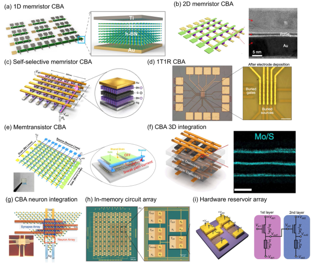
Fig. 4 Memristive array configurations and integrated in-memory circuits. a 1D memristor passive CBA. b 2D memristor passive CBA. c Memristor CBA with access selector devices. d Memristor CBA with access transistor devices. e Self-selective memtransistor CBA. f CBA for 3D integration. g Integration between synapse CBA and neuron devices. h Integrated in-memory circuits and its CBA. i Integrated in-memory circuits for multilayer hardware reservoirs. a Reproduced from [69]. b Reproduced with permission [73], copyright © 2021 Springer Nature Limited. c Reproduced from [47]. d Reproduced from [89]. e Reproduced with permission [86], copyright © 2021, American Chemical Society. f Reproduced from [90]. g Reproduced with permission [103], copyright © 2020 WILEY‐VCH Verlag GmbH & Co. KGaA, Weinheim. h Reproduced from [121]. i Reproduced with permission [85], copyright © 2022 Wiley‐VCH GmbH |
4.1.2 2D Memristor Passive CBA
4.2 Memristor CBA with Access Selector or Transistor
4.3 Multiterminal Memtransistor CBA
4.4 3D Integration
4.5 Integration for In-memory Circuits
4.5.1 Synapse CBA Integration with Neurons
4.5.2 In-memory Circuit Design
5 Functionality and Performance Evaluation
5.1 Basic Functionalities Based on 2D Materials
5.1.1 Pattern Memorization
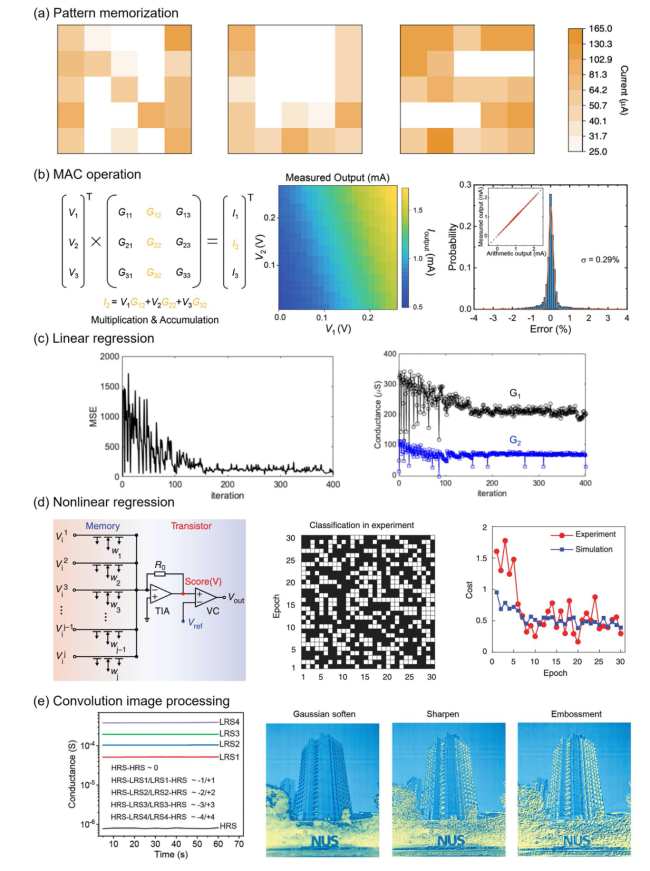
Fig. 5 Fundamental functionalities of memristive arrays. a Pattern memorization based on a 5 × 5 PdSe2 memristor array. b MAC operation based on a 3 × 3 HfSe2 memristor array. c Linear regression using a 2 × 1 h-BN array. d Nonlinear regression with activation function using WSe2 synaptic transistors and activation circuits. e Convolution image processing using a 6 × 3 PdSe2 memristor array. a Reproduced with permission [73], copyright © 2021 Springer Nature Limited. b Reproduced with permission [71], copyright © 2021 Wiley‐VCH GmbH. c Reproduced from [69]. d Reproduced with permission [101], copyright © 2021, The American Association for the Advancement of Science. e Reproduced from [38] |
5.1.2 MAC Operation
5.1.3 Linear Regression
5.1.4 Nonlinear Regression
5.1.5 Image Processing
5.2 System-Level Implementation of Neural Network Applications
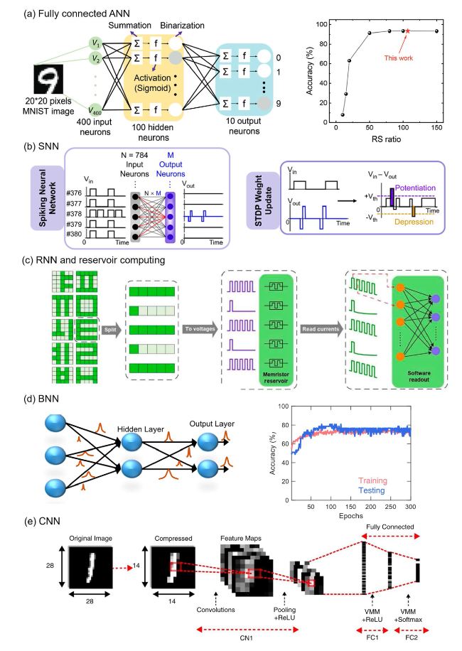
Fig. 6 System-level implementation for neural network applications. a Fully connected neural networks for MNIST dataset pattern recognition using HfSe2-based memristors. The right panel shows the relationship between offline classification accuracy and the HfSe2-based memristor RS ratio. b SNN for MNIST pattern recognition using MoS2-based memtransistors. c RNN and reservoir computing using SnS-based memristor for language recognition. d BNN for prediction of PIMA diabetes dataset using MoS2-based memtransistors. e CNN for MNIST dataset pattern recognition using MoS2-based memristors. a Reproduced with permission [71], copyright © 2021 Wiley‐VCH GmbH. b Reproduced with permission [100], copyright © 2021, American Chemical Society. c Reproduced from [81]. d Reproduced from [102]. e Reproduced from [90] |


