HIGHLIGHTS
1 Introduction
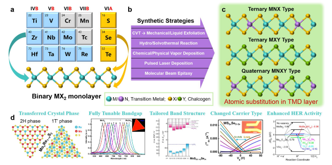
Fig. 1 a Construction of binary TMD monolayer, b synthetic strategies for atomic substitution in TMD layer, c representative structures after partial modification of metal (M, N) or/and chalcogen (X, Y) atoms in TMDs, and d tunable/enhanced properties and improved performance provided by atomic substitution in TMD layers |
2 Concepts and Rules for Atomic Substitution in TMDs
Table 1 Description and comparison of functionalizations on 2D TMDs and their impacts |
| Functionalizations | Involved species | External ratio | Description | Enhanced properties and performances |
|---|---|---|---|---|
| Doping | TMDs and other elementsa | < 10% | Trace amount of atoms in lattice or surface adsorption | Changed carrier type/density; limited tuning of bandgap and band structure; high reactive ability |
| Hybridization | Different types of TMDs; TMDs and other nanomaterials (0D to 2D) | 20-80% | Vertical/lateral heterostructure via stacking, surface adsorption or covalent linkage | New channel for separating and transferring carriers; high catalytic activity |
| Atomic substitution | Ternary or quaternary TMDs | 0-100% | Uniform random solid solution; structural integrity and homogeneousness | Modulated crystal phase; continuously tunable bandgap; tailored band alignment/structure; controlled carrier type/density; adjusted electroconductibility; increased surface activity |
a The choice of element for incorporation into TMDs can be virtually any element from the Periodic Table of Elements, with the exception of elements belonging to the same or adjacent group as the elements presented in the TMDs |
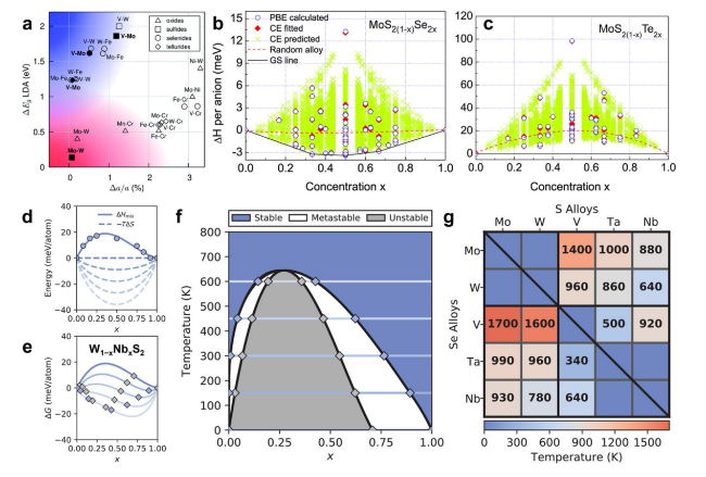
Fig. 2 Principles/rules and theoretical guidance for synthesizing ternary TMDs. a Lattice constant matching for metal-metal pairs of 2H TMDs based on lattice constants. The shaded blue area in the top left corner is populated with vanadium-molybdenum and vanadium-tungsten dichalcogenides, which are metal-semiconductor alloys. The shaded pink area in the bottom left corner contains semiconductor-semiconductor alloys of molybdenum and tungsten dichalcogenides. Reproduced with permission from Ref. [65]. Copyright 2014, Royal Society of Chemistry. Calculated mixing enthalpies for b MoS2(1−x)Se2x and c MoS2(1−x)Te2x via different simulation methods (all symmetry-inequivalent alloy configurations in a 24-atom cell are used for the calculation by CE). Reproduced with permission from Ref. [66]. Copyright 2013, AIP Publishing. d DFT-calculated and fitted mixing enthalpy (ΔHmix, solid line) of W1−xNbxS2, along with the entropy contribution (ΔS, dashed line) to the free energy at temperatures between 0 and 600 K. e x-dependent free energy of W1−xNbxS2 obtained by merging the enthalpy and entropy terms from d. f Horizontal lines “one-to-one” correspond with the free energies in e for revealing stability. The blue and gray diamonds correspond to boundary points between different stability regions in the equilibrium phase diagram. g Miscibility temperatures of all the 20 MNX- and 5 MXY-type TMDs in the 2H phase. The top right and bottom left triangles correspond to sulfide and selenide TMDs, respectively, while the diagonal corresponds to MXY-type TMDs. Dark blue spaces indicate miscible TMDs. Reproduced with permission from Ref. [68]. Copyright 2020, Wiley-VCH |
3 Strategies and Approaches for Atomic Substitution in TMD Layers
3.1 Liquid Exfoliation
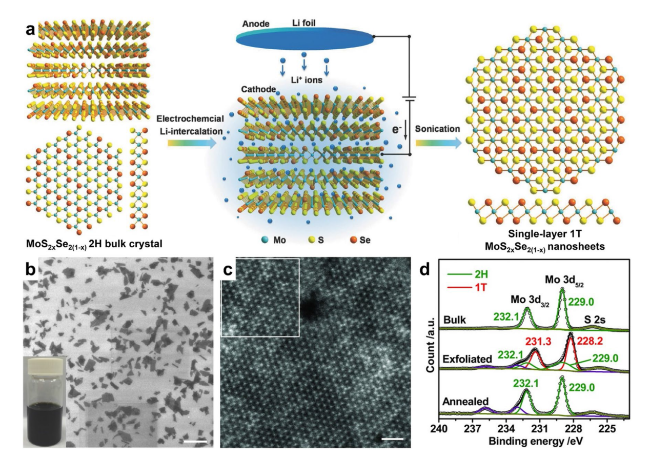
Fig. 3 Li-ion intercalation-assisted liquid exfoliation of 2H-phase MoS2xSe2(1−x) bulk crystal to form 1T-phase MoS2xSe2(1−x) monolayer. a Schematic illustration for preparing single-layered MoS2xSe2(1−x) nanosheets. b-d Characterization of MoS2xSe2(1−x) nanosheets for demonstrating the formation of 1T-phase in the exfoliated MoS2xSe2(1−x) nanosheets: b SEM image of exfoliated high-concentration MoS2xSe2(1−x) nanosheets (scale bar, 2 µm). c Atomic STEM image of a typical MoS2xSe2(1−x) nanosheet with 1T-phase (scale bar, 1 nm). d High-resolution XPS Mo 3d spectrum of 2H-phase MoS2xSe2(1−x) bulk crystal, and the exfoliated (1T) and annealed (2H) MoS2xSe2(1−x) nanosheets. Reproduced with permission from Ref. [80]. Copyright 2016, Wiley-VCH |
3.2 Hydrothermal and Solvothermal Reaction
Fig. 4 a Schematic diagram for the synthesis of Mo1−xNbxSe2 nanosheets through one-pot solvothermal reaction using MoCl5, NbCl5, (PhCH2)2Se2 as precursors with different ratios and oleylamine as solvent. b HRTEM image for showing the assembly of nanosheets into flower-like spheres. c HAADF-STEM image and EDX elemental mapping of Mo (L shell), Nb (L shell), and Se (L shell) for Mo0.5Nb0.5Se2. Reprinted with permission from Ref. [93]. Copyright 2021, American Chemical Society |
3.3 Chemical Vapor Deposition
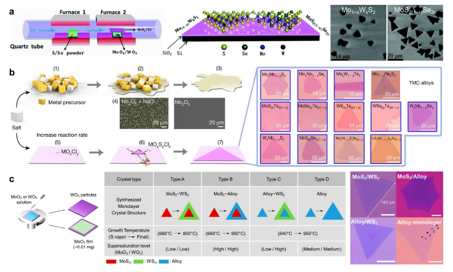
Fig. 5 Schematic diagrams of a typical CVD process for the controllable fabrication of high-quality ATMD monolayers. a Typical tube-furnace set-up employed for the growth of ternary monolayers (left figure), the two-dimensional structures of Mo(1−x)WxS2 monolayer and MoS2(1−x)Se2x monolayer (middle figure), and the corresponding SEM morphology of Mo(1−x)WxS2 and MoS2(1−x)Se2x (right figure). Reprinted with permission from Ref. [95]. Copyright 2015, Royal Society of Chemistry. b Proposed process for decreasing the melting point of the precursors after the addition of salt, the growth process of the 2D atomic layer, and the optical images of 13 ATMD layers synthesized using the molten-salt-assisted CVD method. The SEM images of the Nb nucleus with and without salt are also presented. Right figures are optical images of 13 ATMD layers synthesized using the molten-salt-assisted CVD method. Reprinted with permission from Ref. [33]. Copyright 2018, Nature Publishing Group. c Solution-processed precursor deposition for the CVD growth of MoS2/WS2 lateral heterostructures and alloys (left), the reaction conditions for the CVD growth of each monolayer structure (middle), and the optical images of each monolayer structure (right). Reprinted with permission from Ref. [106]. Copyright 2019, American Chemical Society |
3.4 Physical Vapor Deposition and Other Strategies
Table 2 The strength and weakness of different bottom-up strategies |
| Parameters | Hydro/solvothermal reaction | CVD | PLD | MBE |
|---|---|---|---|---|
| Uniformity | Medium | High | High | High |
| Controllability | High | High | High | High |
| Scalability | Medium | High | High | High |
| Efficiency | Medium | High | Medium | Medium |
| Cost effectiveness | High | Medium | Medium | Low |
4 Diverse Characteristics of Multinary TMDs
4.1 Varied Crystal Structures of Multinary TMDs
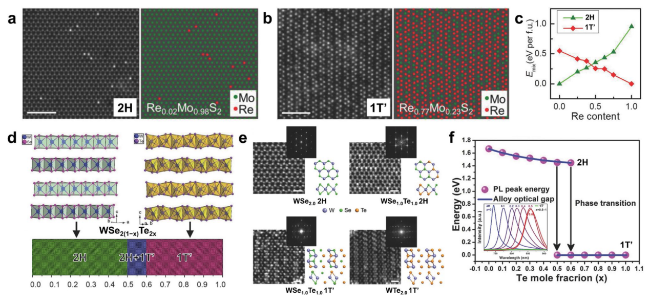
Fig. 6 Transition of crystal phase in 2D ATMDs. a-b Structure of RexMo1−xS2 monolayers at different Re concentrations, as shown in the experimental STEM-ADF images (left) paired with the corresponding atom mapping images (right). To enhance clarity, S atoms are excluded from the atom mapping images. c Calculated mixing/formation energy in 2H- and 1T’-phase RexMo1−xS2 alloy at different Re concentrations. Reproduced with permission from Ref. [120]. Copyright 2018, Wiley-VCH. d Crystal structure of 2H WSe2 and 1T’ WTe2, along with the composition-dependent phases in WSe2(1−x)Te2x. e Atomic resolution STEM characterization of WSe2(1−x)Te2x (x = 0-1) monolayers with different Te concentration. Z-contrast STEM images reveal the atomic structure of pristine WSe2 monolayer in the 2H phase, alloyed WSe1.0Te1.0 monolayer in the 2H phase, alloyed WSe1.0Te1.0 monolayer in the 1T’ phase, and monolayer WTe2 in the 1T’ phase. Corresponding FFT patterns are shown in the inset. f Composition-dependent band gaps (x) and the photoluminescence spectra (PL, inset) of the monolayer WSe2(1−x)Te2x alloys. Reproduced with permission from Ref. [48]. Copyright 2016, Wiley-VCH |
Table 3 Atomic substitution-induced phase transition in special ternary TMDs |
| Ternary TMDs | Phase transition as x increases | Turning point of phase transition | Refs |
|---|---|---|---|
| Mo1−xRexSe2 | 2H→1T’ | ~ 0.42 | [47] |
| WSe2(1−x)Te2x | 2H→1T’ | ~ 0.5-0.6 | [48] |
| Mo1−xVxSe2 | 2H→1T | ~ 0.7 | [54] |
| WTe2xS2(1−x) | 2H→1T’ | ~ 0.45 | [74] |
| RexMo1−xS2 | 2H→1T’ | ~ 0.5 | [120] |
| W1−xVxSe2 | 2H→1T | ~ 0.7 | [121] |
| W1−xRexS2 | 2H→1T’ | ~ 0.4375 | [124] |
| Nb1−xVxSe2 | 2H→1T | ~ 0.3 | [126] |
4.2 Fully Tunable Bandgaps of Multinary TMDs
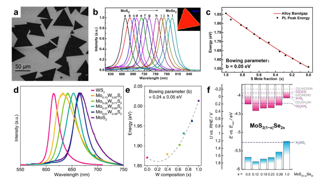
Fig. 7 Composition-dependent band gap/edge in ATMDs. a Typical SEM morphology of the CVD-synthesized MoS2xSe2(1−x) nanosheets. b PL spectrum of the MoS2xSe2(1−x) nanosheets and a typical PL mapping of a single ternary nanosheet (inset) excited with a 488-nm laser. c Composition (x)-dependent bandgaps of the alloy nanosheets. Reproduced with permission from Ref. [44]. Copyright 2014 American Chemical Society. d PL spectra of Mo1−xWxS2 monolayers with the controlled compositions. e Measured optical bandgap of Mo1−xWxS2 monolayers (x = 0-1). Reproduced with permission from Ref. [131]. Copyright 2021, American Chemical Society. f Electronic band structures of few-layer MoS2(1−x)Se2x films, with all energetic levels relative to the reduction potentials (vs. RHE) for aqueous CO2 reduction reaction (pH = 6.8). The valence band edges are derived by XPS, while optical band gaps are measured via ellipsometry. Reprinted with permission from Ref. [132]. Copyright 2020, American Chemical Society |
4.3 Composition-dependent Raman Scattering of Multinary TMDs
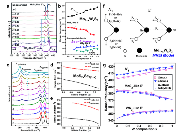
Fig. 8 Composition-dependent Raman scattering in ATMD monolayers. a Raman spectra of Mo1−xWxS2 monolayers with different W compositions. The three blue lines show frequency shift of E’ and A1’ peaks with W composition. b Composition-dependent Raman frequencies of Mo1−xWxS2 monolayers. Reprinted with permission from Ref. [142]. Copyright 2014, Royal Society of Chemistry. c Raman spectrum of MoS2xSe2(1−x) nanosheets excited with a 488-nm argon ion laser. d-e Raman shift of S-Mo related modes [E2g(S-Mo), A1g(S-Mo)] and Se-Mo related modes [A1g(Se-Mo), E2g(Se-Mo)] as S mole fraction. Reproduced with permission from Ref. [44]. Copyright 2014, American Chemical Society. f Schematic illustration of displacing atoms for the Raman active E’ and A1’ modes in Mo1−xWxS2 monolayer and force constants used in MREI model. g Composition-dependent Raman frequencies of E’ and A1’ (E2g1 and A1g for bulk) modes in Mo1−xWxS2 alloys. The solid and dashed lines represent the fitting results of Mo1−xWxS2 monolayers and bulks via the MREI, respectively, while the scattered square and triangle points are the experimental data of Mo1−xWxS2 monolayers and bulks, respectively. Reprinted with permission from Ref. [142]. Copyright 2014, Royal Society of Chemistry |
5 Improved Performances of Multinary TMDs
5.1 Electronic Devices
5.1.1 Regulated Carriers in Type and Density
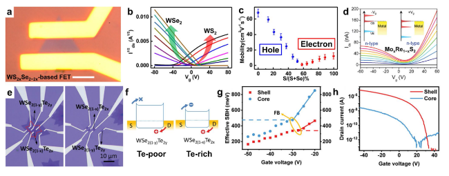
Fig. 9 Composition-dependent electronic properties in ternary TMDs. a-c Electrical transport of WS2xSe2−2x nanosheets: a optical microscopy of a typical back-gated field-effect transistor made of a WS2xSe2−2x nanosheet (scale bar, 5 μm), b transfer characteristics (Id1/2-Vg plot) of WS2xSe2−2x nanosheet transistors with different S atomic ratios from nearly pure WSe2 (brown curve) to nearly pure WS2 (black curve), and c field-effect mobility vs S atomic ratio in WS2xSe2−2x alloy nanosheets, where the blue dots represent the hole mobility in WSe2-rich alloys and red dots represent electron mobility in WS2-rich alloys. Reproduced with permission from Ref. [46]. Copyright 2015, American Chemical Society. d Transfer curves (Ids-Vg) of Mo0.98Re0.02S2 alloy FET, which presents a “bipolar-like” conduction behavior. Reproduced with permission from Ref. [45]. Copyright 2020, Wiley-VCH. e-h Electrical characterization of WSe2−2xTe2x/WSe2−2yTe2y core/shell structure-based transistors: e optical image of the core/shell structure-based transistors. f Band alignments of core and shell transistors along the channel. The shell WSe2−2yTe2y (Te poor) transistor has smaller hole Schottky barrier to facilitate hole transport, while the core WSe2−2xTe2x (Te rich) has more balanced electron/hole Schottky barriers to favor ambipolar transport. g Effective Schottky barrier height as a function of gate voltage for shell and core transistors. h Electrical transport properties of the homogeneous transistors. The homogeneous shell transistor shows strong p-type transport, while the core transistor displays ambipolar behavior. The difference between the core and shell regions can be attributed to the bandgap difference between these two materials. Reproduced with permission from Ref. [157]. Copyright 2020, Wiley-VCH |
5.1.2 Enhanced Electronic Performances
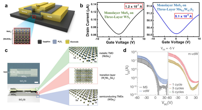
Fig. 10 Improved device performance using ATMDs as interfaces. a-b Current enhancement and bipolar current modulation of top-gate transistors based on monolayer MoS2 on three-layer WxMo1−xS2: a schematic illustration of the top-gate transistor. The gate electrode is separated from the conducting channel by an insulating layer of Al2O3. The panel shows the layer structure of the channel material, which is composed of monolayer MoS2 grown on MoxW1−xS2. b ID-VGS curves of the devices with monolayer MoS2 on three-layer WS2 (left) and Mo0.3W0.7S2 (right), respectively. The voltage VDS was set to 2 V for all measurements. Reprinted with permission from Ref. [158]. Copyright 2018, American Chemical Society. c-d The interfacial transition region of WxNb1−xSe2 for lowering the potential barrier height between the WSe2 channel and NbSe2 electrode in the WSe2-based bottom-gate FET with NbSe2 electrode: c optical image and schematic drawing of WSe2-based bottom-gate FET with NbSe2 electrode (scale bar, 100 μm). d Transfer characteristics (IDS-VBG) of FET devices with different electrode-channel structures: MS (metal-semiconductor, Pd-WSe2), vdW (NbSe2-WSe2), and m-vdW (mixed layer containing NbSe2-WxNb1−xSe2-WSe2): 1, 3, and 5 cycle junction devices. Data were fitted by averages and standard deviations of 10 devices with each junction type. IDS was measured at VDS of − 5 V in devices with channel length of 50 μm and width of 100 μm. Reproduced with permission from Ref. [153]. Copyright 2016, American Chemical Society |
5.2 Optoelectronic Devices
5.2.1 Modulated Defect/Trap Levels
Fig. 11 Enhanced photoelectronic performance of ternary TMDs over binary TMDs, making MoS2(1−x)Se2x a promising candidate for use in industrial applications in nanophotonic devices. a Photograph of a large-scale, continuous multilayer MoS1.15Se0.85 film on a 4-inch quartz wafer. b Schematic illustration of MoS1.15Se0.85-based visible light photodetectors, including 20 devices with identical geometry. c Suggested band diagrams with localized defect states for MoS2, MoS1.15Se0.85, and MoSe2. d Plots of photocurrent of MoS2, MoSe2, and MoS1.15Se0.85 as a function of bias voltage. e Device-to-device variations in photocurrent extracted from 20 devices for MoS2-, MoSe2-, and MoS1.15Se0.85-based photodetectors. Reprinted with permission from Ref. [163]. Copyright 2019, Wiley-VCH |
5.2.2 Anisotropic and Broadening Photoresponse
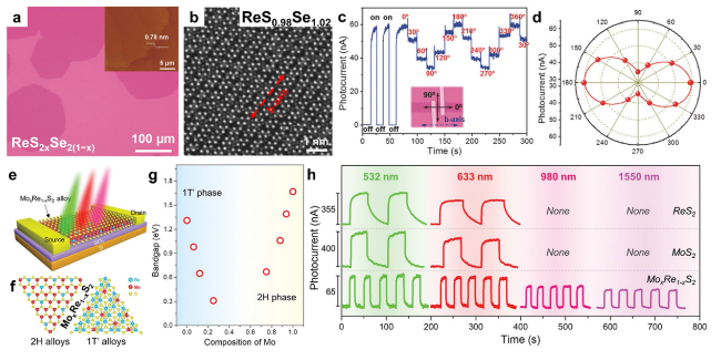
Fig. 12 Anisotropic and broadened photoresponse. a-d Anisotropic photoresponse provided by ReS2xSe2(1−x) alloys: a typical optical microscopy of monolayer ReS2xSe2(1−x) alloys on SiO2/Si substrate and AFM image of as-grown ReS2xSe2(1−x) alloys on mica substrate (inset). b ADF-STEM image of monolayer ReS0.98Se1.02 alloy. c Photocurrent response of ReS1.06Se0.94 device under light on and off irradiation, and the light with different polarization direction. The direction of b-axis is determined via ARPRS (angle-resolved polarized Raman spectra). d Polar plots for the photocurrent with respect to the polarization angle of the incident light. Reproduced with permission from Ref. [130]. Copyright 2017, Wiley-VCH. e-h Broadened photoresponse provided by MoxRe1−xS2 alloys: e schematic diagram for the photoelectric measurement of the MoxRe1−xS2 alloy device. f Atomic structure of 2H and 1T’ MoxRe1−xS2 alloys. g Plots of bandgap as a function of the Mo composition x. h Plots of bandgap as a function of the Mo composition x. i Photocurrent as a function of time for ReS2 (the first row), MoS2 (the second row), and MoxRe1−xS2 alloy (the third row) devices under light illumination with different wavelength: 532, 633, 980, and 1550 nm. The photoresponse measurements of these devices were taken at Vds = 2 V, Vg = 0 V, the laser power density is ~ 5 mW mm−2. Reproduced with permission from Ref. [45]. Copyright 2020, Wiley-VCH |
5.3 Electrocatalytic Hydrogen Evolution Reaction
5.3.1 Enhanced Catalytic Activity by 2H-Phase Ternary TMDs
5.3.2 Enhanced Catalytic Activity by 1T/1T’-Phase Ternary TMDs
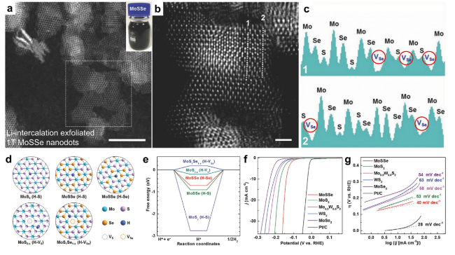
Fig. 13 Enhanced HER performance provided by Li intercalation-exfoliated 1T-phase MoSSe nanodots. a Atomic resolution L2D-WF-filtered HAADF-STEM of MoSSe nanodots. Inset in a: photograph of aqueous solution of MoSSe nanodots (scale bar, 5 nm). b Enlarged L2D-WF-filtered image of MoSSe nanodots shown in the dotted square in a (scale bar, 1 nm). c Brightness profiles along the dotted lines in b. VSe in the brightness profiles represents the Se vacancy. d Atomic models for hydrogen atoms adsorbing at the active sites of basal planes of 1 T-phase MoS2, 1T-phase MoSSe, 1T-phase MoS2 with S vacancy, and 1T-phase MoSSe with Se vacancy. e Calculated free energy versus the reaction coordinates of HER for the basal planes of various catalysts. f iR-corrected polarization curves of Li intercalation-exfoliated 1T-phase MoSSe, MoS2, Mo0.5W0.5S2, WS2, and MoSe2 nanodots, and the commercial Pt/C catalysts. g The corresponding Tafel slopes of these catalysts derived from f. Reproduced with permission from Ref. [53]. Copyright 2018, Wiley-VCH |
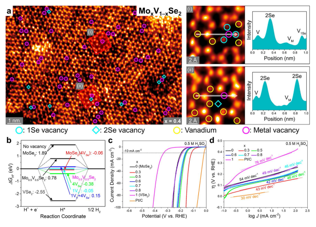
Fig. 14 Enhanced HER performance provided by vacancy-rich Mo1−xVxSe2 nanosheets. a Atomically resolved HAADF-STEM images of vacancy-rich Mo0.6V0.4Se2 (with intensity profile along the white line). The darker regions contain the V vacancies (marked by magenta circles). The V atom sites are labeled by yellow circles, and the Se vacancies (1Se: monovacancy, 2Se: divacancy) are marked by cyan circles and diamonds, respectively. In the line profiles, VM and V1Se represent the metal vacancy and Se monovacancy sites, respectively. b Gibbs free energies (ΔGH*) for x = 0, 0.5, and 1 with different vacancy structures. c LSV curves with scan rate of 2 mV s−1 for Mo1−xVxSe2 and Pt/C catalysts in 0.5 M H2SO4. d Tafel plots derived from the LSV data measured at low potential region. Reproduced with permission from Ref. [54]. Copyright 2021, American Chemical Society |
Table 4 Comparison of HER performance of diverse TMDs with different morphologies and crystalline phases with their corresponding end-materials |
| 2D (A)TMDs | Synthetic methods | Morphology | Phase | Tafel slope | Overpotential | References |
|---|---|---|---|---|---|---|
| MoS0.98Se1.02 | CVD | Monolayer films | 2H | 119 | 273 | [134] |
| MoS2 | 2H | 134 | 335 | |||
| MoSe2 | 2H | 134 | 303 | |||
| MoSSe | Li-ion intercalation | Nanodots | 1T | 40 | 140 | [53] |
| MoS2 | 1T | 53 | 173 | |||
| MoSe2 | 1T | 54 | 209 | |||
| ReSSe | Li-ion intercalation | Nanodots | 1T’ | 50.1 | 84 | [169] |
| ReS2 | 1T’ | 106.9 | 320 | |||
| ReSe2 | 1T’ | 50.8 | 123 | |||
| WS1.14Se0.86 | CVD | Triangular monolayer nanosheets | 2H | 85 | 80 | [59] |
| WS2 | 2H | 95 | 100 | |||
| WSe2 | 2H | 100 | 150 | |||
| rGO/W0.4Mo0.6S2 | Wet chemical method | Heterojunction thin films | 2H | 38.7 | 96 | [170] |
| rGO/WS2 | 2H | 68.4 | 150 | |||
| rGO/MoS2 | 2H | 82.0 | 197 | |||
| Mo0.37W0.63S2/C | CVD | Membranes | 2H | 53 | 137 | [143] |
| MoS2/C | 2H | 68 | 178 | |||
| WS2/C | 2H | 60 | 166 | |||
| Re0.55Mo0.45S2 | CVD | Monolayer flakes | 1T’ | 56 | 147 | [120] |
| ReS2 | 1T’ | 200 | 438 | |||
| MoS2 | 2H | 134 | 475 | |||
| MoS2 | 1T | 77 | 216 | |||
| Re0.9Mo0.1Se2 | Hydrothermal reaction | Nanosheets | 1T’ | 42 | 77 | [55] |
| ReSe2 | 1T’ | 61 | 107 | |||
| MoSe2 | 2H | 77 | 188 | |||
| Mo0.5Nb0.5Se2 | Solvothermal reaction | Nanosheets | 2H | 46 | 140 | [93] |
| MoSe2 | 2H | 56 | 207 | |||
| NbSe2 | 2H | 85 | 292 | |||
| Mo0.7V0.3Se2 | Colloidal reaction | Nanosheets | 2H | 43 | 114 | [54] |
| MoSe2 | 2H | 54 | 195 | |||
| VSe2 | 1T | 76 | 330 | |||
| Nb0.7V0.3Se2 | Colloidal reaction | Nanosheets | 2H/1T | 72 | 236 | [126] |
| NbSe2 | 2H | 86 | 295 | |||
| VSe2 | 1T | 107 | 386 | |||
| W0.9V0.1Se2 | Colloidal reaction | Nanosheets | 2H | 80 | 128 | [121] |
| WSe2 | 2H | 83 | 168 | |||
| VSe2 | 1T | 108 | 387 |
The Tafel slope is measured in mV dec−1 and the overpotential is measured in mV at j = 10 mA cm−2 |
5.4 Other Applications
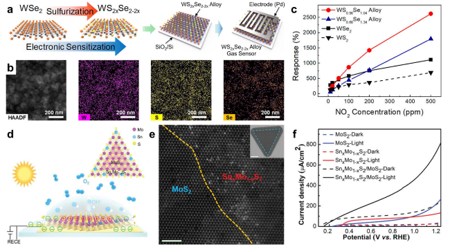
Fig. 15 a-c Enhanced gas-sensing performance provided by WS2xSe2−2x layers: a schematic for the fabrication process of the WS2xSe2−2x alloy-based gas sensors. b HAADF TEM image of WS0.96Se1.04 alloy and EDS elemental maps of W, S, and Se in HAADF images. c Response of WSe2, WS0.66Se1.34 alloy, WS0.96Se1.04 alloy, and WS2 gas sensor for NO2 exposure as a function of gas concentration. Reproduced with permission from Ref. [127]. Copyright 2018, American Chemical Society. d-e Enhanced photoelectrocatalytic performance provided by SnxMo1−xS2/MoS2 heterostructure as a photoanode: d schematic illustration of the photoelectrocatalysis measurements. The SnxMo1−xS2/MoS2-on-quartz sample was connected in the external circuit with Ti electrodes. All the measurements were taken in 0.5 M Na2SO4 solutions. The light illumination was produced using a 300-W Xe lamp unless otherwise specified. Inset in d: atomic structure diagram of the lateral SnxMo1−xS2/MoS2 heterostructure. e Atomic resolution STEM image taken from the epitaxial metal-semiconductor heterostructure at the interface. The yellow dotted line indicates the atomic interface. Inset is a typical SEM image of SnxMo1−xS2/MoS2 heterostructure. f Linear-sweep voltammogram curves of different anodes. Solid line: light irradiation. Dashed line: dark. Reprinted under the terms of the Creative Commons Attribution License from Ref. [172]. Copyright 2020, The Authors, published by Wiley-VCH |
6 Emerging Janus Ternary TMD Monolayers
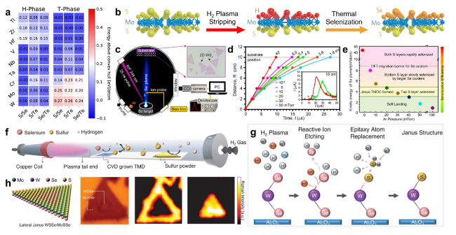
Fig. 16 Strategic preparation of Janus TMDs. a Thermodynamic stability of the H-phase and T-phase for different Janus XMY monolayers. The colors denote the energy above the convex hull in eV/atom. Reprinted with permission from Ref. [178]. Copyright 2019, American Chemical Society. b Synthesis of the Janus SMoSe monolayer. A MoS2 monolayer grown by CVD is exposed to H2 plasma to strip the top-layer S. The plasma is then switched off, and a quartz boat loaded with Se powder is moved next to the SMoH sample without breaking the vacuum. Se powders are then thermally vaporized to achieve selenization and complete the synthesis of Janus SMoSe monolayers. Reprinted with permission from Ref. [50]. Copyright 2017, Nature Publishing Group. c-e PLD-based low-energy implantation into 2D TMDs to form Janus structures: c experimental setup for Se plasma generation and impingement on CVD-grown WS2 monolayer within a vacuum chamber equipped with an ICCD camera and a translatable probe for ion-flux measurement. d R-t plots of the leading edge of the plasma (from ion probe currents, see * in inset) track the propagation and deceleration in different background Ar pressures. e Summary diagram of KE regimes for selenization of WS2 monolayer by using Se PLD. Selenization of only the top S layer of WS2 monolayer suitable for Janus SWSe formation occurs between 20 and 40 mTorr for Se plume KEs between 3 and 4.5 eV atom−1. At low pressures (≤ 20 mTorr) and plume KEs above 5.4 eV atom−1, selenization of the bottom S layer by larger Se clusters increases and completes rapidly once pressures decrease toward vacuum. Reproduced with permission from Ref. [182]. Copyright 2020, American Chemical Society. f-h Room-temperature synthesis of 2D Janus TMDs. f Schematic demonstration of the selective epitaxy atomic replacement (SEAR) process through inductively coupled plasma for the synthesis of 2D Janus TMDs. g Working scheme of room-temperature SEAR process. h The atomic representation and optical image of Janus SMoSe/SWSe lateral heterostructures, and Raman mapping at 290 and 284 cm−1 for characteristic Janus SMoSe and SWSe peaks. Reproduced with permission from Ref. [101]. Copyright 2020, Wiley-VCH |
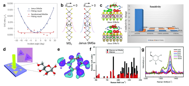
Fig. 17 Characterization of built-in dipole moment in JTMD layers and ultrasensitive detection of organic molecules/biomolecules. a Angle-dependent SHG intensity ratio between p and s polarization in the Janus SMoSe and randomized alloy samples. The Ip/Is ratio (blue circles) increases symmetrically with more tilted incidence and is fitted well by an angle-dependent SHG model (blue curve). The Ip/Is ratio (red circles) undergoes almost no change as the incident angle varies, and the flat fitting (red curve) suggests a negligible out-of-plane dipole. Reprinted with permission from Ref. [50]. Copyright 2017, Nature Publishing Group. b Schematics of the crystalline structure (side view) of MS2 and Janus SMSe (M = Mo, W) and the corresponding wave functions of electron (fe) and hole (fh) in excitons in each material. Reprinted with permission from Ref. [174]. Copyright 2021, American Chemical Society. c Calculated electron density difference (EDD) plots of acetone adsorption on S layer of Janus SMoSe and SMoTe monolayers. Green and red represent the regions of electron depletion and accumulation, respectively. Reprinted with permission under a Creative Commons Non-Commercial No Derivative Works (CC-BY-NC-ND) Attribution License from Ref. [184]. Copyright 2020, American Chemical Society. d-g SERS-based ultrasensitive detection of glucose by Janus SMoSe: d optical image of Janus SMoSe and schematic of laser irradiation of glucose on Janus SMoSe for SERS characterization. The scale bar is 20 μm. e-f DFT calculations for the glucose molecule on the Janus substrate. e Charge distribution in glucose. The light blue and the purple regions show the electron cloud distribution in the isolated single glucose molecule and in anchored glucose on Janus SMoSe, respectively. Their distinguishing shapes indicate the drastic charge redistribution after glucose is adsorbed on monolayer Janus SMoSe. f Calculated Raman peaks for isolated glucose and anchored glucose on Janus SMoSe. g Concentration-dependent Raman spectra of glucose on Janus SMoSe. The integrated peak intensity increased linearly with elevated glucose concentration in solution. Reprinted with permission from Ref. [185]. Copyright 2020, Royal Society of Chemistry |


