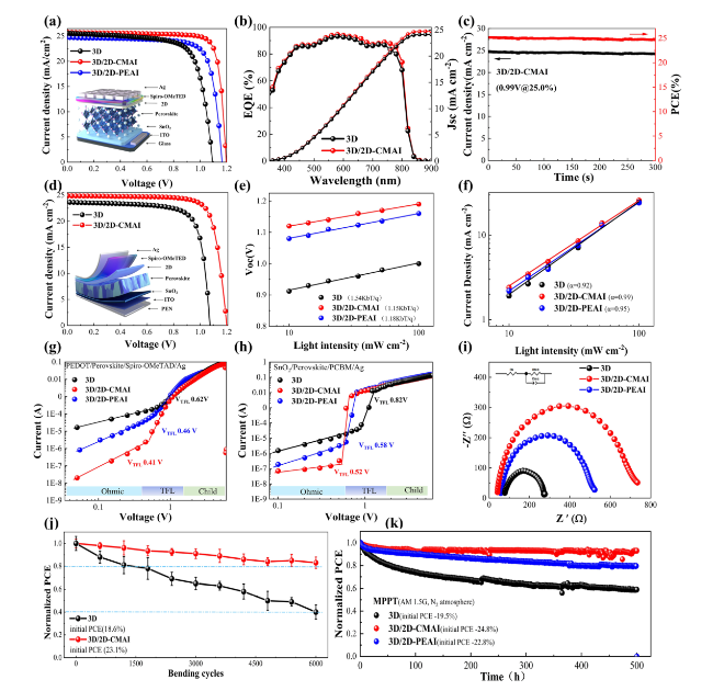
To evaluate the effect of organic cations with different structural rigidities on the photovoltaic performance of PSCs, PSCs with the device architecture of ITO/SnO
2/3D/2D/Spiro-OMeTAD/Ag were constructed and tested under simulated 1 sun illumination at an intensity of 100 mW cm
−2 (AM 1.5 spectrum). The details of the deposition process are described in the experimental section. The optimal concentrations of CMAI and PEAI are first determined from Tables S2 and S3. The current density-voltage (
J-
V) characteristics of the leading devices are shown in
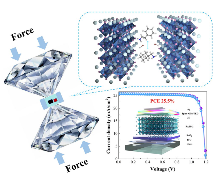
Fig. 5a, and the photovoltaic performances are summarized in Table S4. The control device shows PCE of 20.2% with short-circuit current (
JSC) of 25.4 mA cm
−2, open-circuit voltage (
VOC) of 1.09 V, and fill factor (
FF) of 72.38%. With the incorporation of the 2D-PEAI phase, the PCE exhibits an improvement of 22.4%, which can be attributed to the passivation effects of the 2D-PEAI as discussed previously. Therefore, a significantly improved
VOC (1.16 V) is observed due to the suppressed non-radiative recombination losses, while a slightly decreased
JSC (24.69 mA cm
−2) might be attributed to the inhibited carrier transport by the bulky organic spacer. For 3D/2D-CMAI-based PSCs, the PCE is further increased to 25.5%, with simultaneously improved
VOC to 1.19 V,
JSC to 25.73 mA cm
−2, and
FF to 83.09%. This achievement stands out as one of the highest reported PCEs to date. Figure S16 and Table S5 show the forward and reverse scan
J-
V characteristics of the champion PSC based on 3D and 3D/2D-CMAI, which exhibits a negligible 0.67% hysteresis index in 3D/2D-CMAI, but increases to 2.6% in 3D. Three-dimensional/2D-CMAI significantly reduces the hysteresis. The EQE of PSCs based on 3D and 3D/2D-CMAI are compared in
Fig. 5b. The integration of these efficiencies provides the
JSC of 24.45 and 24.73 mA cm
−2, respectively, consistent with the
J-
V characteristics. Based on the previous characterizations, the presence of structurally flexible CMA
+ abates the carrier and phonon coupling strength, which might decrease the associated electron capture by the defect states, in addition to chemical passivation on the halide or lead vacancies, thus increasing the defect tolerance of perovskite. It ultimately minimizes the SRH losses and gives rise to an exceptional
VOC value of 1.20 V (the highest
VOC in this work as shown in Table S2). We observed that this is one of the highest
VOC records achieved for narrow bandgap FAPbI
3 perovskite to date. The device was then tracked at the maximum power point for 300 s, and the stabilized power output is presented to be 25.0% (
Fig. 5c), which aligns well with the
J-
V characteristics.


