In order to investigate the effects of the Ti
0.936O
2 nanocrystals on the optical and electronic properties of the TiO
2 ETLs, the optical bandgap of Ti
0.936O
2@TiO
2 films were first evaluated by ultraviolet-visible (UV-vis) absorption spectra and corresponding Tauc plots. The results show that the embedding of Ti
0.936O
2 enables slight increase in the bandgap of the TiO
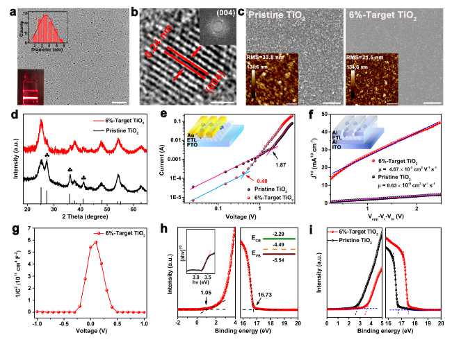
2 ETLs from 3.20 to 3.22 eV, with insignificant change on the optical transmittance, as shown in Figs. S9 and S10. To evaluate the electronic properties, the defect density (
Nt) and the electron mobility (
µ) of the TiO
2 ETLs were successively examined by the space charge-limited current (SCLC) method. The result shows that the embedding of Ti
0.936O
2 results in the reduction of
Nt from initial 6.48 × 10
16-1.39 × 10
16 cm
−3 (
Fig. 1e and Table S1), which may be due to the improved crystallization kinetics of TiO
2 and the high-quality ETLs. Moreover, the
µ is found to be boosted by two orders of magnitude from pristine 8.63 × 10
-5-4.67 × 10
-3 cm
2 V
−1 s
−1 for the 6%-target TiO
2 ETLs (
Fig. 1f), which is consistent with the conductivity (
σ) result that indicates higher
σ for 6%-target TiO
2 due to a large slope (Fig. S11). The improved electronic properties are mainly attributed to the construction of Ti
0.936O
2@TiO
2 p-n homojunction, which is evidenced by an inverted “V-shape” with typical p-n junction feature from the Mott-Schottky plot shown in
Fig. 1g [
18]. To confirm the p-type characteristic of the Ti
0.936O
2, the ultraviolet photoelectron spectroscopy (UPS,
Fig. 1h) was used to check its electronic structure of the Ti
0.936O
2. Based on the optical bandgap (3.25 eV) (inset in
Fig. 1h), the corresponding Fermi energy level, the conduction band energy level and the valence band energy level are calculated to be − 4.49, − 2.29, and − 5.54 eV, respectively, which identifies the p-type semiconductor feature of the Ti
0.936O
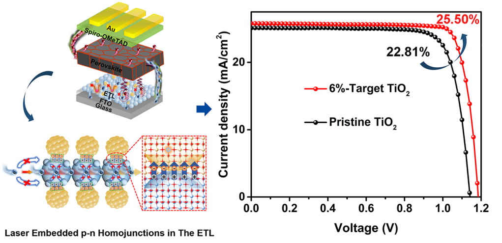
2 nanocrystals. Such p-n construction greatly accelerates the carrier transport at both the surfaces and the boundaries of TiO
2 particles to restrain carrier loss owing to the increase of the depletion width [
18,
19]. It is also found that the embedded p-n homojunction is helpful to improve electronic structure of TiO
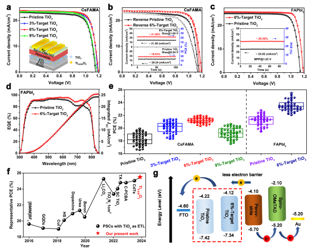
2 ETLs with upward-shifted energy level, enabling a better energy level alignment with top perovskite active layer to lower the interfacial electron barrier (
Figs. 1i and S12) [
9]. Detailly, the UPS characterization of laser-processed Ti
0.936O
2 nanocrystals strongly confirms their p-type semiconductor characteristic (
Fig. 1h), which were embedded into the n-type TiO
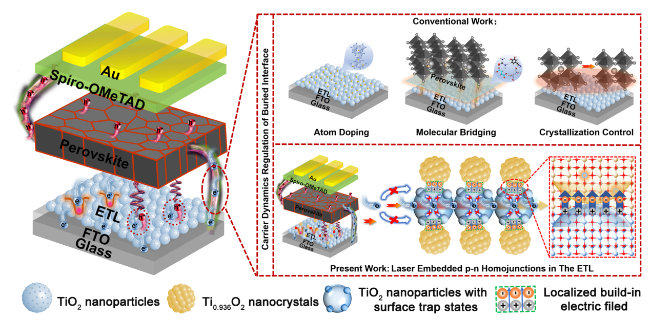
2 matrix to form a p-n junction by generating a uniform Fermi level (Fig. S12b). It is worth noting that the formed p-n homojunctions between Ti
0.936O
2 and TiO
2 could create numerous localized built-in electric fields with a direction from n-type TiO
2 to p-type Ti
0.936O
2, as shown in
Scheme 1 and Fig. S12b, which enables not only the effective promotion of carrier transport at both the surfaces and boundaries of TiO
2 matrix due to the expansion of the depletion width [
19], but also the oriented transport of photo-generated charge carriers, which favors for the boosted electron mobility (
Scheme 1) [
10].


