
1. Introduction
Rapid Single-Flux-Quantum (RSFQ) circuit technology is a type of superconducting digital circuit technology based on the superconducting Josephson effect. The signal is stored in the superconducting loop in the form of magnetic flux quantum and transmitted in the form of a single flux quantum pulse (SFQ pulse) [1].
Stochastic Computing (SC) theory, as a low-cost computing theory, was proposed in the 1960s [2]. Different from the traditional computing theory, the “stochastic number (SN) stream” is used as the representation of the data. The value of data corresponds to the probability of “1” in the SN stream. In recent years, due to their small size, low power consumption, and high fault tolerance, SC circuits have been widely used in machine learning [3], image processing [4], communication engineering [5], digital filtering [6] and other fields.
In this paper, we propose a Finite Impulse Response (FIR) filter based on the RSFQ circuit. As a basic digital filter, the FIR filter has a wide range of applications in communication systems. The nature of the RSFQ circuit makes it possible to greatly reduce energy consumption at a high clock frequency (even up to 770 GHz [7]). However, implementing FIR filters requires a large number of adders and multipliers, which is hard to realize using the RSFQ circuit due to the current fabrication process constraints. In order to maximize the use of high-speed and low-energy characteristics of RSFQ circuits, SC theory is adopted in the proposed FIR filter. We designed a novel stochastic number generator (SNG), a stochastic-to-binary converter (SBC), and an FIR filter based on the RSFQ circuit and verified via logic simulation.
The remainder of this paper is organized as follows. Section 2 describes the SC theory. Section 3 describes the microarchitecture of the proposed filter. Section 4 describes the logic design. Section 5 shows the simulation results. Section 6 discusses and evaluates the result of our design. Section 7 concludes the paper.
2. Stochastic computing
2.1. Computing method
In SC circuits, the value of data is represented by the probability of “1” in an SN stream. For example, “11001010” and “00001111” both represent 0.5.
As shown in Fig. 1, multiplication operation is realized by “bit-wise AND” in SC by only using a logical AND gate. However, the result is not completely precise if the input SN streams are not completely independent. Assume that A and B are random events. If the probability of A and B occurring simultaneously is equal to the product of the probability of each occurrence, then A and B are independent of each other. That is, if P(AB)=P(A) P(B), the events A and B are said to be independent of each other, referred to as A and B independent. In the SC circuits, the “scaled addition” method is used to process the addition operation. Here is an ideal example as shown in Fig. 2, note that the addition result can be reduced by any possible value between 0 and 1, but converges to the expected value (i.e., 1/2 of the sum of the two inputs) in the case of long enough SN streams.
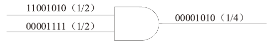
Fig. 1. Diagram of SC multiplication. |

Fig. 2. Diagram of SC addition. |
2.2. Correlation of SN streams
As previously stated in subSection 2.1, the accuracy of SC circuits is highly dependent on the independence of the SN streams, which is typically determined by the correlation of SNGs. One common method for generating SN streams is through the use of linear feedback shift registers (LFSRs) as the stochastic source. However, due to the pseudo-random nature of LFSRs, using the same LFSR design in multiple computing circuits results in highly correlated SN streams. To mitigate this issue, while still allowing for design reuse, the application of time delay on the output of the LFSR has been proposed as a solution. In order to further investigate the correlation of SN streams from the same LFSR with different time delays, the autocorrelation of m-sequences, which are the output of the LFSR, was computed and is presented in Fig. 3. The results indicate that implementing time delay effectively reduces the correlation of SN streams from different ports, thus providing evidence for the feasibility of this method for improving the accuracy of SC circuits.

Fig. 3. Correlation of m-sequence. |
2.3. Pros and cons
The advantages and disadvantages of the SC circuit are as follows:
1) Advantages:
•Low hardware cost. In comparison to traditional computation circuits that require large multipliers and adders, SC circuits can achieve the same function with only a single logic gate and a multiplexer.
•Strong fault tolerance. In SN streams, there is no concept of the least significant bit (LSB) and the most significant bit (MSB) as all bits are equally significant. This avoids the problem of large errors occurring when the noise occurs at the MSB.
2) Disadvantages:
•Imprecise computing. Because of the length of the SN streams we adopted, there inevitably are some errors during the calculation.
•Large processing delay. As precision increases, the computation time for the SC process will grow exponentially. For example, if the precision is increased from 4 bits to 5 bits, the length of the SN stream will increase from 16 (24) to 32 (25).
3. Microarchitecture
For digital filters based on SC theory, the order N cannot be increased without limit. Because as the filter order increases, the amount of data under processing increases, so the correlation between input data increases, resulting in the deviation rate of the output data increasing [2]. After weighing the performance of the filter and the deviation rate of SC, we adopt a 4th-order for the proposed filter. In the engineering field, a filter with a 4th-order can be used as a time domain equalizer in a communication system, which has practical value.
The 4th-order FIR digital filter can be expressed by the following formula:
$y(n)=h 0 \bullet x(n)+h 1 \bullet x(n-1)+h 2 \bullet x(n-2)+h 3 \bullet x(n-3)$
here, x(n) and y(n) are the input and output discrete signal sequences. n means the time point, n ∈ [0, +∞). h0, h1, h2 and h3 are the parameters of FIR filter.
The microarchitecture of the proposed FIR filter is shown in Fig. 4, where “SPL” denotes a splitter. Suppose the system clock period is T. Take an SC circuit in 4-bit precision as an example. The length of an SN stream is 15 (24-1). Outputting one bit (0 or 1) of an SN stream from SNG requires time T, so outputting a whole SN stream corresponding to a binary number (BN) stream from SNG requires 15T. Therefore, the sampling frequency of our digital signal processing system should be 1/15T. The Nyquist frequency of the designed filter is half of the sampling frequency, which is 1/30T.
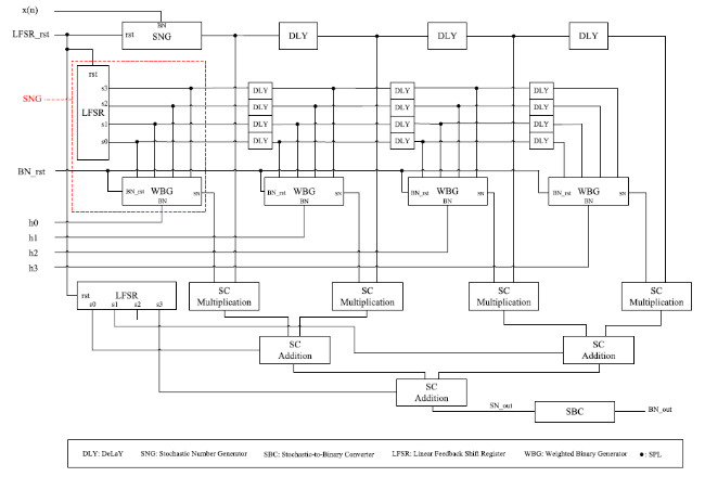
Fig. 4. Microarchitecture of the proposed FIR filter. |
In Fig. 4, the data synchronized by DLY blocks are in the form of SN streams. The time to update one SN stream is 15T, which is essentially 15 consecutive cycles T to output a “0” or “1” signal. As is mentioned in Section 2.2, to avoid the correlation of LFSR output streams, 1T latency is needed to reduce the correlation of four WBGs. Similarly, the output of LFSR is input to SC addition modules as their selection port. In order to reuse the LFSR, all the selection ports are connected to the same LFSR (the bottom left one in Fig. 4) but different output ports to implement a kind of time latency to avoid correlation.
The data from WBG are the SN stream corresponding to the filter parameters $h_{0} \sim h_{3}$, and the data from SNG are the SN stream corresponding to the input BN stream x(n) to the filter. Every 15 clock cycles x(n) moves to the next stage from left to right; then the filter multiplies x(n) with $h_{0} \sim h_{3}$ in SC Multiplication modules, respectively. After the multiplication, the results flow down to the addition tree (SC Addition modules), finally merge into the SBC, and convert into a BN stream to output.
4. Logic design of FIR digital filter
4.1. Design of SNG
SNG is designed to convert a BN stream into an SN stream. Take the 4-bit SNG as an example, when the value of BN is “5”, the SN contains five “1”s and ten “0”s in the stream. The positions of “1”s are randomly distributed.
SNG is divided into two parts structurally. One is an LFSR to generate SN streams, and the other one is a weighted binary generator (WBG). Fig. 5 shows the logic design of the SNG, where RDFF is an RSFQ DFF cell with a resettable function, and CB is the RSFQ confluence buffer to merge two or three inputs into one output. In RSFQ circuits, XOR and RDFF, like DFF, have a latch function in the cell itself.
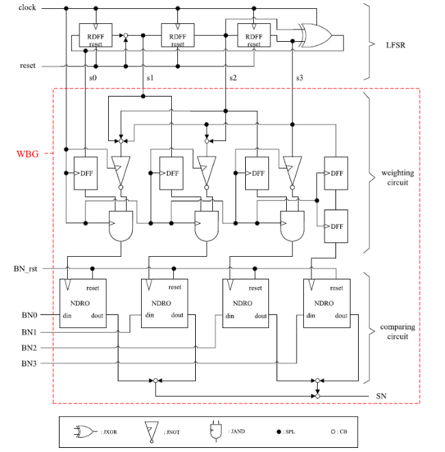
Fig. 5. Logic design of SNG. |
LFSR is used to generate SN streams. Assuming the bit-width is 4, LFSR generates an SN stream in 15T (24-1) with a bit-width of 4 (the range of SN stream is [1⇓⇓⇓⇓⇓⇓⇓⇓⇓⇓⇓⇓⇓-15]). LFSR generates an SN stream to WBG. Only when both the clock ports of the NDROs and BN inputs are “1”, the output of WBG is generated as an SN. The number of “1”s in the SN stream output by LFSR is equal to the value of the BN stream, which realizes the conversion from the BN stream to an SN stream.“Weight” is a binary feature. In a BN stream, the LSB and the MSB have different contributions to the number of “1”s in the SN stream. For 4-bit, the MSB “1” of the BN stream contributes eight “1”s to the SN stream, however, the LSB “1” only contributes one “1” to the SN stream. CBs, NOTs, ANDs, and other RSFQ cells are used to “weight” the BN streams output by the LFSR. For each bit of the BN stream, there is only one output port highlighted in the weighting circuit.
4.2. Design of MUX
MUX is designed to implement SC addition, which contains two input data ports (din0, din1), a selection port (s), and an output data port (dout). The output from dout equals the input to din1 when “1” is input to the s. Reversely, output from dout equals the input to din0 when “0” is input to the s. The state diagram of MUX is shown in Fig. 6. Therefore,
$\text { dout }=s \times \operatorname{din} 1+(1-s) \times \operatorname{din} 0$
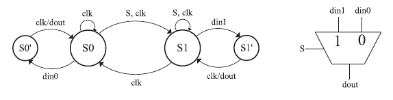
Fig. 6. State diagram of MUX. |
Here, dout, din1, and din0 are all the values of SN streams. When the value of SN stream input to s = 1/2, the formula is simplified as:
$\text { dout }=1 / 2 \times(\operatorname{din} 1+\operatorname{din} 0)$
In fact, Eq. 3 is the addition operation in SC. Fig. 7 shows the logic design of MUX, where the NDRO is the RSFQ Non-Destructive ReadOut logic cell.

Fig. 7. Logic design of MUX. |
4.3. Design of SBC
SBC is designed to convert an SN stream into a BN stream. In fact, SBC can be regarded as a counter. Fig. 8 shows the logic design of SBC. In our design, the width of the SN stream is 15 (24-1), so the corresponding SBC needs to output the count value every 15 clock cycles. As shown in Fig. 8, the upper half is a frequency divider composed of 4 cascaded Resettable T Flip-Flops (RTFFs), which is used to implement the frequency divider. Every 16 clock periods are input to the first RTFF, and the last RTFF outputs one pulse. Therefore, in order to achieve an output every 15 clock periods, the output of the fourth RTFF is fed back to the input of the first RTFF. The lower half of SBC is the counter, composed of 4 cascaded T1 triggers. T1 triggers are similar to “half adders”. Every 15 clock cycles, the divider in the upper half outputs a pulse, thereby resetting the state of T1 trigger and outputting the count value.
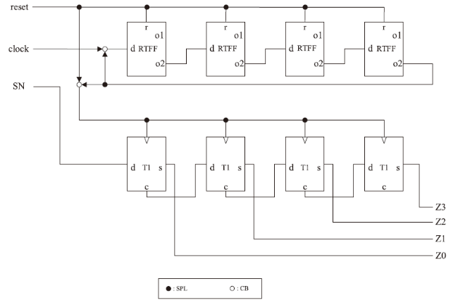
Fig. 8. Logic design of SBC. |
5. Simulation of the FIR filter
We have performed the logic-level simulation of the designed FIR filter with Icarus Verilog [8] and GTKWave software [9]. We used Verilog hardware description language [10] to do the logic-level simulation based on the Open Dataset of CONNECT Cell Library for the 1.0-μm Nb/AlOx/Nb nine-layer advanced process 2 (ADP2) with a critical current density of 10 kA/cm2 [11].
To verify the functionality of the whole design, we have defined several test benches for the proposed FIR filter. Take the calculating path of the parameter h 0 as an example to analyze the correctness of the entire circuit. For the convenience of description, the data flow through the path is marked as “A”, “B”, “C”, “D”, “E”, “F”, and “G”, as shown in Fig. 9. The values of “A” and “B” are 11/15 (101011111101101) and 10/15 (110101111010110), after the multiplier operation (AND gate), “C” is obtained, and its value is 6/15 (100001111000100). “D” (6/15, 001010000011011) is also the output from another multiplier. “C” and “D” are added (scaled addition) to obtain “E” with a value of 6/15 (000011101000101). Similarly, “E” and “F” (1/15, 001000000000000) are scaled-added to obtain “G” (5/15, 001010001000101), and SBC counts “G”. Finally, Z = 0101 (i.e. G = 5/15, 001010001000101) is output, due to the imprecise property of SC. The results show that the proposed FIR filter works correctly at 10 GHz (see Fig. 10).

Fig. 9. Dataflow in the proposed FIR filter. |
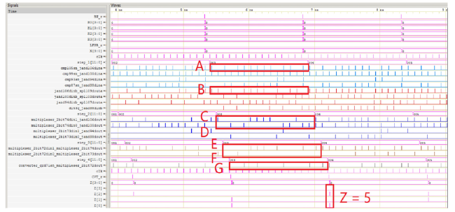
Fig. 10. Simulation results of the proposed FIR filter. |
The theoretical range of the input and output data of the proposed filter is (0,1). However, due to the feature of the “scaled addition” operation, the value of the addition result is reduced to 1/2. Therefore, the output data after the two-stage adders is reduced to 1/4. Unlike the traditional binary computing theory, SC has deviations related to the length and correlation of the SN stream and circuit design.
Considering the proposed filter accuracy is 4-bit, in the case of weighing test validity and simulation duration, we choose 1024 points as the input data length of the proposed filter. Each set of input patterns (input waveforms and filter parameters) generates a set of data graphs. Take the input waveform as a periodic triangle wave and filter parameters $h_{0} \sim h_{3}$ respectively as 11/15, 15/15, 3/15, and 8/15 for an example. The corresponding data graph is Fig. 11. The subfigures (a) and (c) are the time domain and frequency domain representations of input data, respectively. The subfigure (b) shows a comparison between simulation and theoretical output in the frequency domain. The red line represents the simulation output and the blue line represents the theoretical one. The purple part means overlap. The simulation outputs show that our FIR has a similar enhancing effect in low frequency compared with theoretical output but has noise in high frequency. The subfigure (d) demonstrates the theoretical frequency response of the proposed FIR filter under given parameters [11/15,1,3/15,8/15], showing obvious low-frequency enhancement and high-frequency suppression effects.
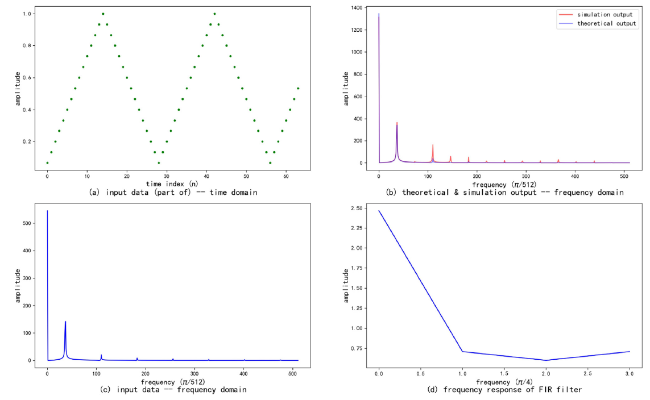
Fig. 11. Data graphs generated by simulation. (a) time domain of input data, (b) frequency domain of theoretical and simulation output, (c) frequency domain of input data, (d) frequency response of FIR filter. |
One of the main parameters for measuring SC is the mean error-to-signal power ratio [6], assuming that the actual output value of the n-th point is $y_{c n}$ and the theoretical output value is $y_{t n}$, the formula is:
$\text { the average error }- \text { to }- \text { signal power ratio }=\frac{1}{N} \sum_{n=0}^{N-1} \frac{\left|y_{c_{n}}-y_{t n}\right|^{2}}{y_{y_{m}}^{2}}$
Table 1. The error of the proposed filter under different parameters and input waveforms. |
| Input waveforms | Input period | Filter Parameters | Average error-to-signal power ratio | |||
|---|---|---|---|---|---|---|
| h0 | h1 | h2 | h3 | |||
| Triangle wave | 28 | 11/15 | 15/15 | 3/15 | 8/15 | 0.0495 |
| Triangle wave | 28 | 11/15 | 0/15 | 2/15 | 14/15 | 0.1010 |
| Triangle wave | 28 | 2/15 | 4/15 | 14/15 | 12/15 | 0.0619 |
| Triangle wave | 28 | 13/15 | 15/15 | 2/15 | 3/15 | 0.1335 |
| Triangle wave | 28 | 5/15 | 9/15 | 15/15 | 11/15 | 0.1411 |
| Square wave | 32 | 11/15 | 0/15 | 2/15 | 14/15 | 0.0249 |
| Square wave | 64 | 11/15 | 0/15 | 2/15 | 14/15 | 0.0162 |
| Random noise | - | 11/15 | 0/15 | 2/15 | 14/15 | 0.1526 |
| Random noise | - | 13/15 | 15/15 | 2/15 | 3/15 | 0.2769 |
It can be seen from Table 1 that the error-to-signal power ratio of the filter is related to the parameters and input waveforms. The parameter values of 11/15, 0, 2/15, and 4/15 result in a low-pass filter response, while the values of 11/15, 15/15, 3/15, and 8/15 result in a more pronounced low-pass filter response at stronger high-frequency rejection. The values of 2/15, 4/15, 14/15, and 12/15, on the other hand, tend to produce a bandstop filter response. It is challenging to implement a high-pass filter using a low-order FIR filter, so the high-pass portion of the experiment was not conducted. Under the same filter parameters, the relationship of deviation rate for different input waveforms is “square wave” < “triangular wave” < “random noise”. “Random noise” is designed for testing the filter in the most extreme case. The smallest error value of the square wave is because there are only two values in the square wave - 15/15 and 1/15. Under different parameters, the error-to-signal power ratio of the filter fluctuates in the range of 0.016 ∼ 0.27.
6. Discussion
We have designed the RSFQ logic circuits of all the components for the proposed FIR filter based on SC theory and simulated the FIR filter at the logic level. It contains 2255 JJs without considering Josephson Transmission Lines (JTLs) and Passive Transmission Lines (PTLs). Table 2 shows that the number of JJs for WBG is much larger than other components. In contrast, the number of JJs for multipliers is the least because multiplication is simple to be implemented using SC theory. Also, the number of DFFs and splitters (SPLs) is larger than in other cells, most of which are used as buffers to synchronize the data and control signals or connect components. The simulation results show it operates correctly at the target frequency of 10 GHz. Under this frequency, it has a very high computing speed, which is 6.67×10⁸ 4-bit filtering computing per second.
Table 2. The number of cells and JJs used in the FIR filter. |
| Components | RDFF | DFF | XOR | NOT | AND | SPL | CB2 | CB3 | NDRO | T1 | RTFF | JJs |
|---|---|---|---|---|---|---|---|---|---|---|---|---|
| LFSRs | 9 | 0 | 3 | 0 | 0 | 30 | 3 | 0 | 0 | 0 | 0 | 243 |
| WBGs | 0 | 25 | 0 | 15 | 15 | 95 | 20 | 5 | 20 | 0 | 0 | 1225 |
| SBC | 0 | 0 | 0 | 0 | 0 | 8 | 1 | 0 | 0 | 4 | 4 | 131 |
| Adders | 0 | 9 | 0 | 3 | 0 | 9 | 3 | 0 | 6 | 0 | 0 | 201 |
| Multipliers | 0 | 0 | 0 | 0 | 4 | 0 | 0 | 0 | 0 | 0 | 0 | 56 |
| Others | 0 | 58 | 0 | 0 | 0 | 17 | 0 | 0 | 0 | 0 | 0 | 399 |
| Total | 9 | 92 | 3 | 18 | 19 | 159 | 27 | 5 | 26 | 4 | 4 | 2255 |
Compared with the FIR filter mentioned in [6] whose 4th-order FIR has an error ratio range from 0.01 to 0.08, the error ratio of our design is from 0.016 to 0.14 for regular waves (triangle waves and square waves) and 0.15 to 0.27 for random noise signals. If we exclude the results of random noise signal experiments, our highest error ratio is only twice the highest error ratio in [6]. Considering the precision of the filter in [6] is 10-bit (that is, the length of SN stream is 1023), whereas 4-bit for our design, at the same system clock frequency, the computing speed of our design is 64 (26) times higher than that of the filter in [6]. Thus, our design realizes a very high computing speed while maintaining an acceptable error ratio.
In addition, our design has a concise structure. Compared with the SBC circuit mentioned in [12], we have a more compact design that saves 4 DFFs in SBC design. In conventional multiplication design, such as [12], an SNG is composed of one LFSR and one WBG. In our design, four SNGs total consist of one LFSR and four WBGs by adopting an LFSR-sharing structure we proposed. That is 171 (3 × 81 - 12 × 6) JJs are saved. According to the discussion in Section 2.2, our design still maintains low correlations in SN streams with the reduction of LFSRs.
However, the proposed FIR filter still has some shortcomings. Firstly, the FIR filter only has 4-bit precision and the order is 4, which is difficult to handle computing tasks that require higher precision and higher order. The higher-order filter leads to longer processing time and increased deviation. The deviation can also be reduced as the length of SN streams increase which also means an increase in data precision. As the length of SN streams increases, the processing time and hardware cost become longer and larger, where we can make a trade-off. Secondly, the Timing constraints in some components are strict. The feedback mechanism is adopted in the frequency divider of the SBC module, which greatly reduces the number of required cells, but it also leads to stricter timing constraints. Thirdly, due to the imprecision of stochastic computing and low-bit quantization of data, it is hard to realize the ideal designing phase characteristic. Therefore, we ignored the phase characteristic design of the FIR filter.
In our design, the unipolar encoding format is adopted, which means a value range of [0,1]. According to [5], if bipolar coding is adopted, the value of the SN stream becomes $(N 1-N 0) / N. N 1$ is the number of 1’s and N0 is the number of 0’s in an SN stream. In the meantime, the SN stream value range also expands to [−1, 1]. The relationship between bipolar-encoded SN stream value Pb and unipolar-encoded SN stream value $P b=2 P u-1$.
7. Conclusion
We have presented the design of an FIR filter with 4-bit resolution utilizing SC technology for an RSFQ circuit, which contains 2255 JJs. The simulation results show it operates correctly at the target frequency of 10 GHz, that is, the sampling frequency of our digital signal processing system is 667 MHz (i.e. Nyquist frequency is 334 MHz). As outlined in the Discussion, our design demonstrates a high computing speed while maintaining a compact structure and a satisfactory level of accuracy.
In future work, we will expand the bit width of the filter and implement more complex functions, such as the sin and cos functions. We will also do experiments on the phase characteristics and fault tolerance of the future filter.
Declaration of Competing Interest
The authors declare that they have no known competing financial interests or personal relationships that could have appeared to influence the work reported in this paper.
Acknowledgment
The authors would like to thank Nagoya University (A. Fujimaki), Yokohama National University (N. Yoshikawa), and AIST (M. Hidaka) in Japan for providing the Open Dataset of CONNECT Cell Library for AIST ADP2.
