

Integrated Circuits and Systems >
Impact of Crack Evolution in Solder Balls on Thermoelectric Model Under Electrical Stress
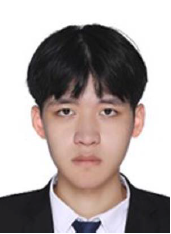 |
KUN HE received the B.Sc. degree in electronic science and technology from the University of Electronic Science and Technology of China, Chengdu, China, in 2022, where he is currently working toward the M.Sc. degree. His research interests include radio frequency (RF) microsystems and advanced packaging technologies. |
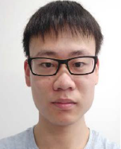 |
HUANPENG WANG received the B.S. degree in electronic information science and technology from Fuzhou University, Fuzhou, China, in 2018, and the M.S. degree in electromagnetic field and electromagnetic waves from the University of Electronic Science and Technology of China, Chengdu, China, in 2021. His research interests include RF circuits, RF microsystems, and advanced packaging technologies. |
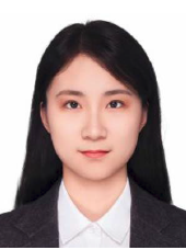 |
YUE TANG received the B.S. degree in communication engineering from Shandong University, Qingdao, China, in 2024. She is currently working toward the M.S. degree in electronic information with the University of Electronic Science and Technology of China, Chengdu, China. Her research interests include radio frequency (RF) microsystems and advanced packaging technologies. |
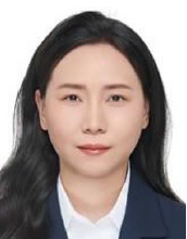 |
JIE LIU received the B.S. degree in electronic information engineering and the M.S. degree in information and system from Beihang University, Beijing, China, in 2004 and 2007, respectively. She is currently working toward the Ph.D. degree. Her research interests include the heterogeneous integration, microsystems, RF circuits, and process design kit (PDK). |
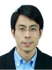 |
MUSHENG LIANG (Senior Member, IEEE) received the B.S. degree in electromagnetic field and microwave communication, the M.S. degree in electromagnetic field, and the Ph.D. degree in microwave technology from the University of Electronic Science and Technology of China (UESTC), Chengdu, China, in 2004, 2008, and 2015, respectively. In 2018, he joined the Department of Physics, UESTC. He is currently the Vice Dean of the Yangtze River Delta Research Institute (Huzhou), UESTC. His research interests include microwave circuits and systems, antenna design, and time-reversal electromagnetics. |
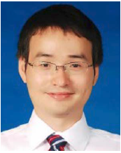 |
YUEHANG XU (Senior Member, IEEE) received the B.S. and M.S. degrees in electromagnetic field and microwave techniques from the University of Electronic Science and Technology of China (UESTC), Chengdu, China, in 2004 and 2007, respectively, and the joint Ph.D. degree from UESTC and Columbia University, New York City, NY, USA, in 2010. In 2010, he joined the Faculty of the Department of Electronic Engineering, UESTC, where he is currently a Professor. He was a Visiting Associate Professor at Case Western Reserve University, Cleveland, OH, USA, in 2016. He is the first author of Equivalent CircuitModeling of Microwave GaN Power Transistors (China Science Press, 2017) and has authored or coauthored more than 150 scientific papers in international journals and conferences. His current research interests include the modeling of radio frequency (RF) electronic devices and microwave integrated circuits. Dr. Xu has been a Technical Program Committee (TPC) Member of IEEE International Conference on Integrated Circuits Technologies and Applications (ICTA) since 2019. He has won three provincial and ministerial science and technology awards since 2016. He was the recipient of the National Natural Science Foundation of China Excellent Young Scholars in 2019. He was the General Chair of MOS-AK in 2019. He was an Associate Editor for International Journal of Numerical Modelling: Electronic Networks, Devices and Fields (IJNM), a Special Issue Guest Editor of Microwave and Optical Technology Letters (MOTL), and an Editorial Committee Member for Research and Progress of Solid-State Electronics and International Journal of High Speed Electronics and Systems. |
Received date: 2024-12-31
Revised date: 2025-01-26
Accepted date: 2025-02-23
Online published: 2025-10-22
Supported by
Key Laboratory of Large-Scale Electromagnetic Industrial Software, Ministry of Education, under Grant(EMCAE202404)
Sichuan Science and Technology Program under Grant(2024NSFJQ0022)
Current thermoelectric models under electrical stress often neglect the critical impact of crack formation, limiting their predictive accuracy for solder ball reliability. To study the impact of cracks under electrical stress conditions, this study designed an electrical stress-induced failure experiment, applying stepwise current loading to the devices under tests (DUTs) to obtain resistance-time curves, with computed tomography (CT) revealing cracks in the solder balls. Based on these experimental results, a thermoelectric coupling model was developed to predict the temperature-resistance relationship of heterogeneous interconnect structures, incorporating crack factors observed during the experiment. The thermoelectric coupling model demonstrated high accuracy, achieving a maximum error of less than 2.5%. By incorporating the effects of crack formation under high electrical stress, the model provides precise predictions of solder ball resistance evolution.
Key words: Electrical stress; solder ball; thermoelectric model
KUN HE , HUANPENG WANG , YUE TANG , JIE LIU , MUSHENG LIANG , YUEHANG XU . Impact of Crack Evolution in Solder Balls on Thermoelectric Model Under Electrical Stress[J]. Integrated Circuits and Systems, 2025 , 2(1) : 36 -45 . DOI: 10.23919/ICS.2025.3547670
| [1] |
|
| [2] |
|
| [3] |
|
| [4] |
|
| [5] |
|
| [6] |
|
| [7] |
|
| [8] |
|
| [9] |
|
| [10] |
|
| [11] |
|
| [12] |
|
| [13] |
|
| [14] |
|
| [15] |
|
| [16] |
|
| [17] |
|
| [18] |
|
| [19] |
|
| [20] |
|
| [21] |
|
| [22] |
|
| [23] |
|
| [24] |
|
| [25] |
|
| [26] |
|
| [27] |
|
| [28] |
|
/
| 〈 |
|
〉 |